
Are you struggling with voids and weak joints in your semiconductor packages? Vacuum soldering might be the solution.
Vacuum soldering removes voids during the soldering process, creating stronger and more reliable connections in semiconductor devices.
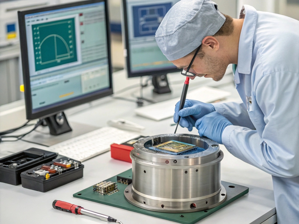
Have you ever wondered how vacuum soldering can improve different semiconductor manufacturing processes? Keep reading, and I'll tell you more about this.
How Vacuum Soldering Applies to Power Device Packaging?
Are your power devices failing due to poor solder joints? Vacuum soldering can improve their reliability.
Vacuum soldering eliminates voids in solder joints of power devices. This improves thermal and electrical conductivity, resulting in better performance.
Power devices, such as MOSFETs and IGBTs, generate a lot of heat during operation. Effective heat dissipation is very important for their reliability and performance. Voids in the solder joints between the power device and the substrate act as thermal barriers, which prevent heat from flowing away from the device. This can lead to overheating and eventual failure.
minimizes void formation by removing trapped gases and volatile substances during the soldering process. The vacuum environment helps to degas the solder material and the surfaces being joined, allowing the molten solder to wet the surfaces completely and create a void-free joint. The result is improved thermal conductivity, lower thermal resistance, and better heat dissipation. This keeps the power device cooler and extends its lifespan.
Here’s a table summarizing the benefits:
Benefit Description
Improved Thermal Conductivity Voids are removed, allowing heat to flow more efficiently from the device to the heat sink.
Reduced Thermal Resistance The thermal path is more direct, reducing the temperature difference between the device and the surroundings.
Enhanced Reliability Lower operating temperatures reduce stress on the device, increasing its lifespan and reliability.
How Vacuum Soldering Applies to MEMS Device Packaging?
Are you having trouble with the delicate packaging of your MEMS devices? Vacuum soldering might be the answer.
Vacuum soldering is ideal for MEMS device packaging. It provides precise control and minimizes contamination, ensuring the reliable operation of these sensitive devices.
MEMS (Micro-Electro-Mechanical Systems) devices are very small and sensitive. Their packaging needs to protect them from the environment while maintaining their performance. Vacuum soldering offers several advantages in MEMS packaging. It provides a clean and controlled environment.
The vacuum environment reduces the presence of contaminants that could affect the functionality of the MEMS device. Also, vacuum soldering allows for precise control of the soldering process. This is very important when dealing with the small sizes and complex geometries of MEMS devices. The absence of voids and the improved joint strength provided by vacuum soldering ensure the long-term reliability of the packaged MEMS device.
Consider these key advantages:
Advantage Description
Clean Environment Reduces contamination, ensuring the MEMS device operates as intended.
Precise Control Allows for accurate placement and bonding of components, which is important for small devices.
Improved Reliability Strong, void-free joints ensure the long-term performance and stability of the MEMS device.
How Vacuum Soldering Applies to Flip Chip Bonding?
Are you struggling with weak connections in your flip chip assemblies? Vacuum soldering can help you achieve stronger bonds.
Vacuum soldering enhances flip chip bonding by removing voids and improving solder joint reliability. This is very important for high-performance electronic devices.
Flip chip bonding is a method of connecting semiconductor dies directly to a substrate. This provides shorter electrical paths and improved performance. However, voids in the solder joints can be a major problem, leading to reduced electrical and thermal conductivity.
Vacuum soldering addresses this issue by eliminating voids during the solder reflow process. The vacuum environment removes trapped gases and volatile substances, allowing the solder to wet the surfaces completely and form a strong, reliable joint. This results in improved electrical performance, better heat dissipation, and increased reliability of the flip chip assembly.
Let's break down the benefits:
Benefit Description
Enhanced Electrical Performance Shorter, reduce resistance and improve signal integrity.
Improved Heat Dissipation Better thermal contact allows for more efficient removal of heat from the die.
Increased Reliability Stronger, more reliable solder joints reduce the risk of failure due to thermal stress or mechanical shock.
How Vacuum Soldering Applies to 3D Packaging?
Are you looking for a reliable way to stack and connect dies in 3D packages? Vacuum soldering might be what you need.
Vacuum soldering enables reliable 3D packaging by creating void-free solder joints between stacked dies. This is very important for high-density electronic devices.
3D packaging involves stacking multiple semiconductor dies on top of each other and connecting them using vertical interconnects. This allows for higher density and improved performance. However, creating reliable solder joints between the stacked dies can be challenging.
Vacuum soldering provides a solution by eliminating voids and improving the quality of the solder joints. The vacuum environment ensures that the solder wets the surfaces completely, creating strong and reliable connections between the dies. This results in improved electrical and thermal performance, as well as increased reliability of the 3D package.
Here’s a look at the advantages:
Advantage Description
High-Density Interconnects Allows for the creation of dense, vertical connections between stacked dies.
Improved Performance Shorter interconnects reduce signal delays and improve overall performance.
Enhanced Reliability Strong,ensure the long-term stability and performance of the 3D package.
How Vacuum Soldering Applies to Hermetic Packaging?
Do you need to ensure that your sensitive components are protected from the environment? Vacuum soldering can help you create a hermetic seal.
Vacuum soldering is used in hermetic packaging to create airtight seals that protect sensitive components from moisture and contaminants. This extends the lifespan and reliability of the devices.
Hermetic packaging is used to protect sensitive electronic components from the harmful effects of moisture, gases, and other contaminants. This is very important for devices that need to operate reliably in harsh environments.
Vacuum soldering can create a hermetic seal by creating that prevent the ingress of contaminants. The vacuum environment ensures that the solder wets the surfaces completely, forming a continuous and airtight seal. This protects the enclosed components from corrosion, degradation, and failure.
Here's what makes it beneficial:
Benefit Description
Environmental Protection Protects sensitive components from moisture, gases, and other contaminants.
Extended Lifespan Prevents corrosion and degradation, increasing the lifespan of the device.
Increased Reliability Ensures reliable operation in harsh environments by maintaining a stable internal environment.
Conclusion
Vacuum soldering improves semiconductor manufacturing by creating stronger, more reliable connections with minimal voids. This technology enhances the performance and lifespan of many electronic devices.