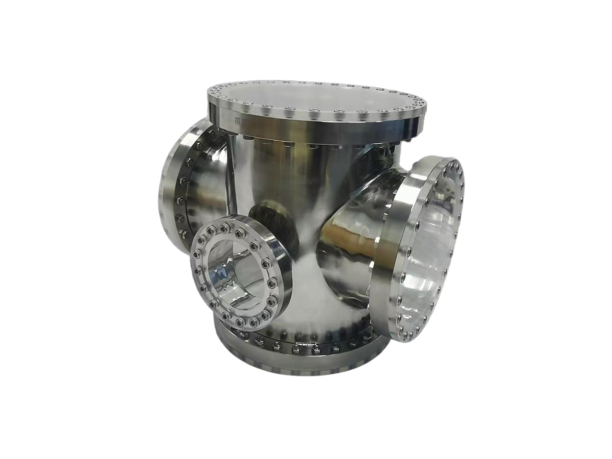
How precise can the surface treatment be? – This question is being redefined with semiconductor industry advances toward the 8nm chip era. With this, an Ultra-High Vacuum (UHV) Chamber is not just a structural component. It’s a decisive factor in a cleaner surface treatment environment with tighter process control.
As semiconductor nodes are becoming increasingly microscopic, advanced surface treatment in the UHV chamber, where most of the critical processes of 8nm manufacturing take place, is no longer a secondary consideration. It directly impacts the particle generation control, outgassing rate, and long-term process stability.
A nanoscopic surface imperfection that may look trivial can lead to particle contamination and directly affect yield. For industries like semiconductor equipment manufacturers, wafer fabrication plants, and scientific research institutions, microscopically accurate surface treatment is non-negotiable.
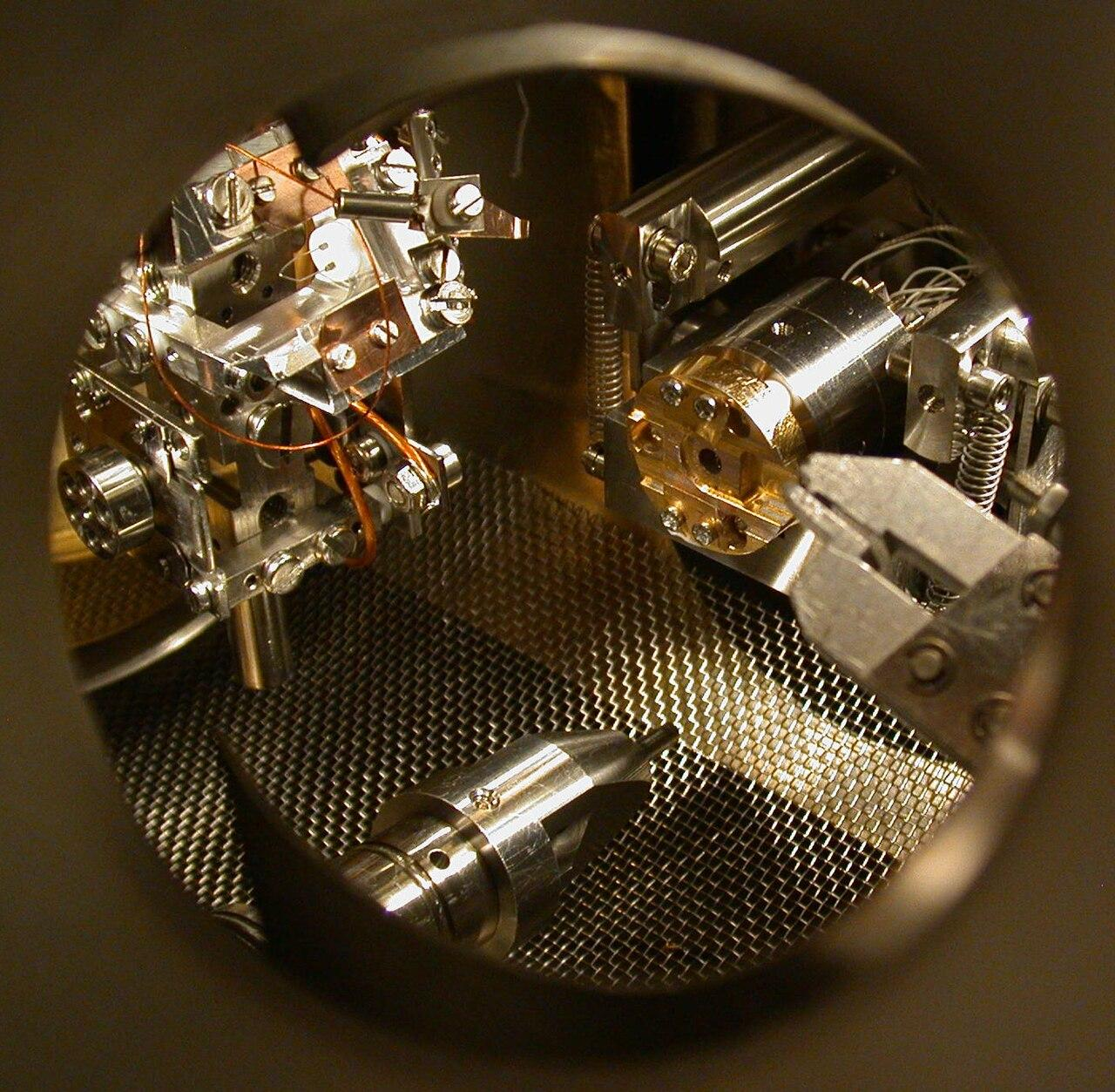
Image source: Kristian Molhave, Wikimedia Commons (CC BY-SA 2.5)
So today we’ll reveal how Laiku meets 8nm process requirements with its advanced polishing, coating, and contamination-control technology on an Ultra-High Vacuum chamber surface.
Why is Ultra-High Vacuum Chamber Surface Treatment Important for 8nm Manufacturing?
8nm manufacturing is increasingly more challenging than the manufacturing of other visible objects. At such a microscopic level of semiconductor manufacturing, even contamination at the atomic level from the surrounding environment can affect yield. So ultra-high vacuum chambers are a must for microscopic semiconductor manufacturing.
But even if pumps create a UHV chamber, the untreated surface inside the chambers is enough to make the 8nm manufacturing faulty. It can release water molecules, metal impurities, hydrocarbons, etc. This is why Ultra-High Vacuum chamber surface treatments have become a strategic way to manufacture microscopically accurate equipment.
There are several critical processes such as Atomic Layer Deposition (ALD), Physical Vapor Deposition (PVD), Chemical Vapor Deposition (CVD), and Advanced Metrology that essentially require an ultra-high vacuum environment. UHV chamber surface treatment brought a breakthrough in modern surface treatment technology for a stable and contamination-free environment for 8nm semiconductor manufacturing.
Advanced Surface Treatment Strategies to Meet 8nm Process Requirements
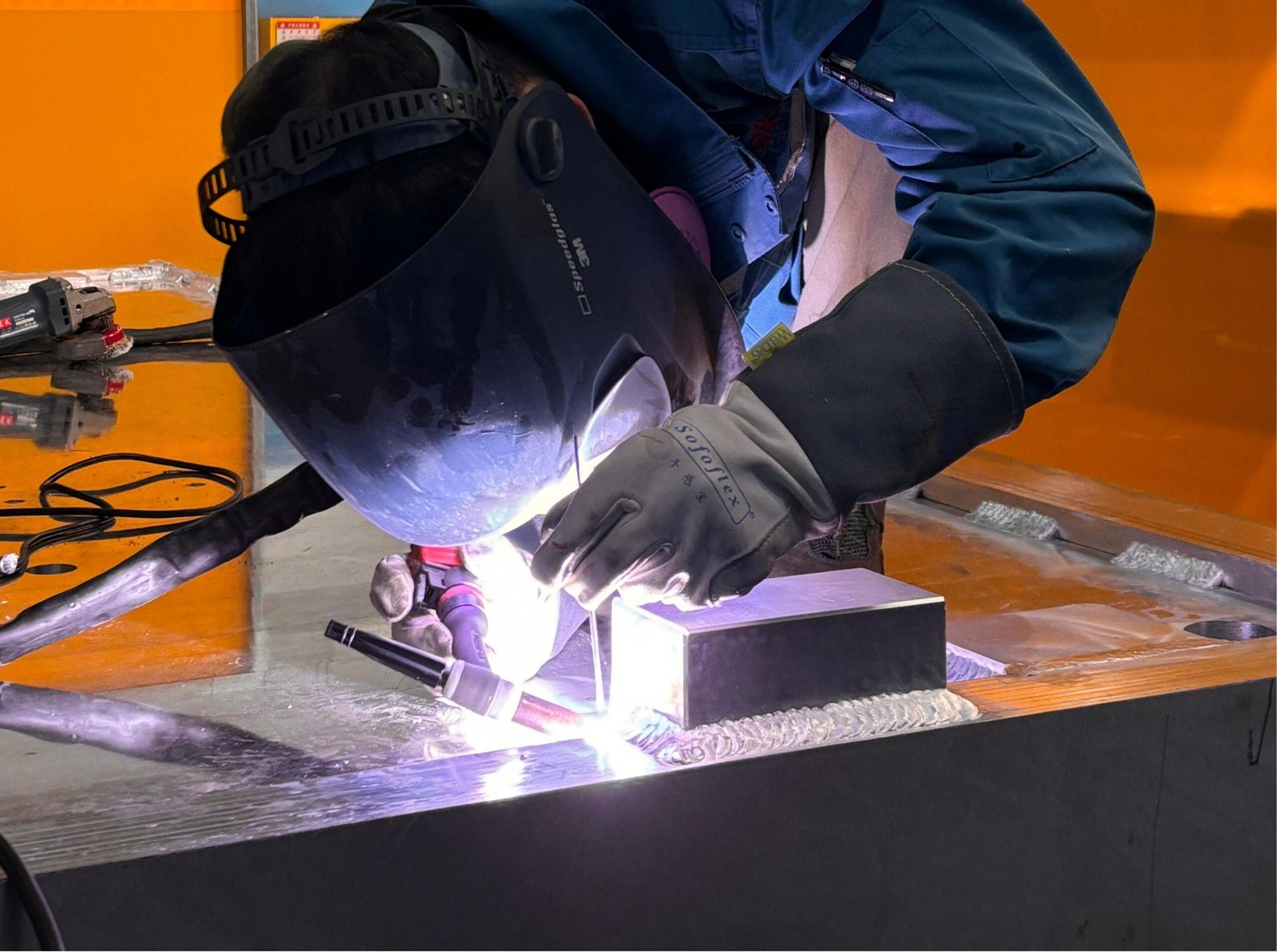
1. Mechanical and Chemical Polishing with Precision
For the surface treatment, the preparation usually starts with mechanical and chemical polishing to make the UHV chamber surface microscopically smooth. If the surface is macroscopically and microscopically rough, the absorption sites are minimized. This can also cause more downstream treatments.
For surface treatment in UHV environments, the surface roughness is targeted below 0.2 micrometers. For critical components, the roughness is targeted to be less. For UHV application, surfaces with finer finishes are achieved with mechanical and chemical polishing.
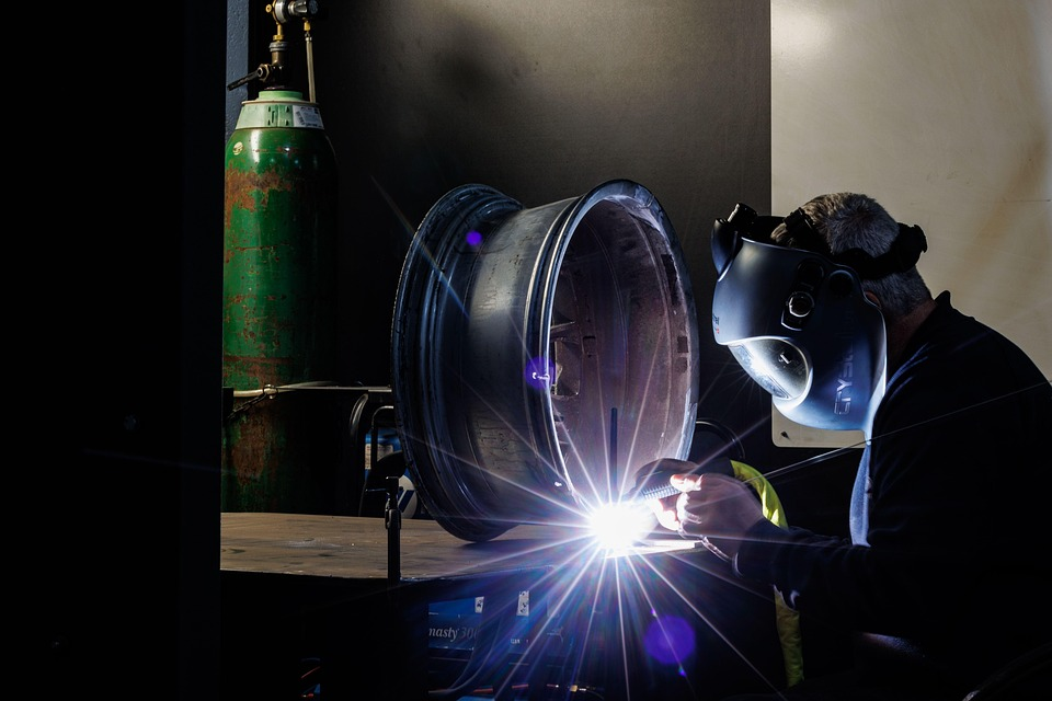
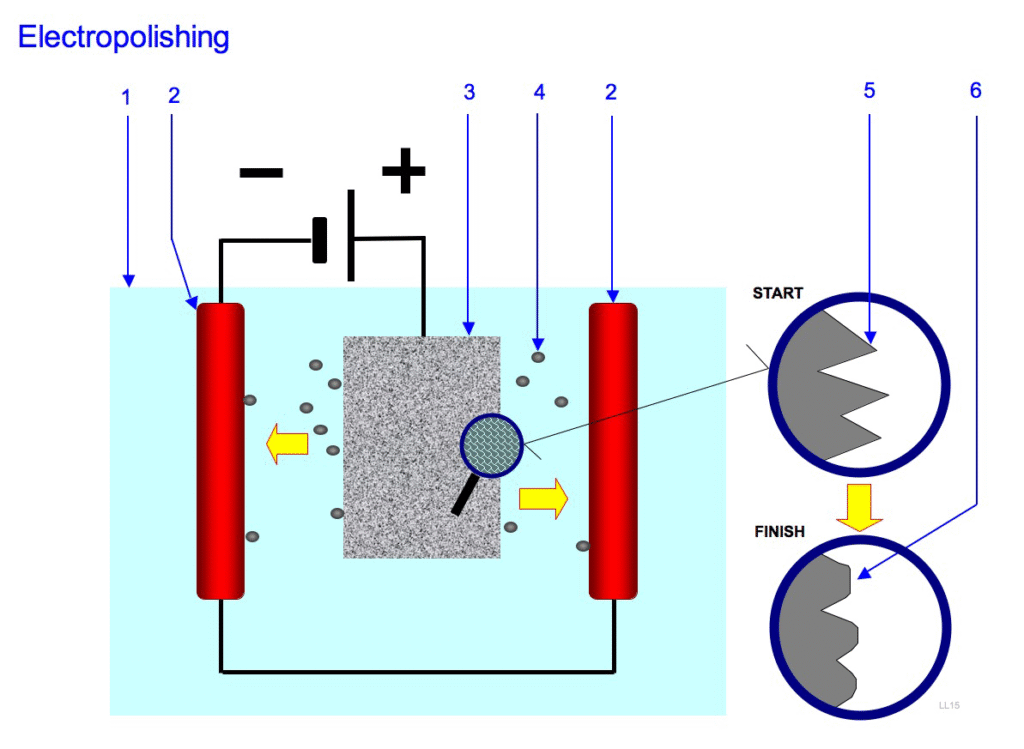
2. Electropolishing for Ultra Smoothness
Electropolishing has become a standard surface treatment for not just UHV chambers, but also other internal components. The purpose of this advanced surface treatment is to achieve extraordinary surface smoothness of the chamber.
This reduced surface roughness eventually leads to a very low outgassing and gas absorption rate. Electropolishing provides 8nm manufacturing processes with a more stable and repeatable environment specifically during processes that require long runs.

Image source: LaurensvanLieshout, Wikimedia Commons (CC BY-SA 2.5)
3. Thermal Bake-out and Desorption Control
From the untreated surface of the UHV chamber, water molecules, hydrocarbons, and other metal impurities are released. This problem is called outgassing which can cause serious contamination. Even one atomic layer of these elements can affect yield for manufacturing a microscopic scientific element like an 8nm semiconductor node.
To solve this problem, thermal bake-out is done on the surface. In this way, the chamber is heated under vacuum condition which leads to the desorption of absorbed water and volatile elements, and is removed by the pumping system. The UHV chamber surface with proper thermal bake-out has a lower base pressure and a faster pump-down rate.
4. Plasma-Based Surface Cleaning
Plasma-based surface cleaning is used for removing hydrocarbons after maintenance or UHV chamber opening. This technique uses plasmas of Oxygen, inert gas, or hydrogen.
With plasma, organic residues and other surface contaminants are removed without disassembling the full machine. Plasma-based UHV surface cleaning in a controlled way increases a high cleanliness level without causing any damage to the surface of the UHV chamber.
Image source: Reginvels, Wikimedia Commons (CC BY-SA 4.0)
5. Advanced Dry and Chemical Surface Treatment
To make the Ultra-High Vacuum chamber surface stable and non-reactive for 8nm manufacturing requirements, a new modern way of surface treatment is to modify the chamber surface chemistry at the atomic level. These treatments include hydrogen-based and passivation processes which make the crystallographic structures more stable.
Eventually, due to this, the chamber surface turns out to be less reactive with the environment. For 8nm manufacturing, where even a microscopic reaction of the semiconductor part with the chamber surface can cause a faulty node, advanced drying and chemical surface treatment of the UHV chamber make it more stable to accurately manufacture an 8nm semiconductor.
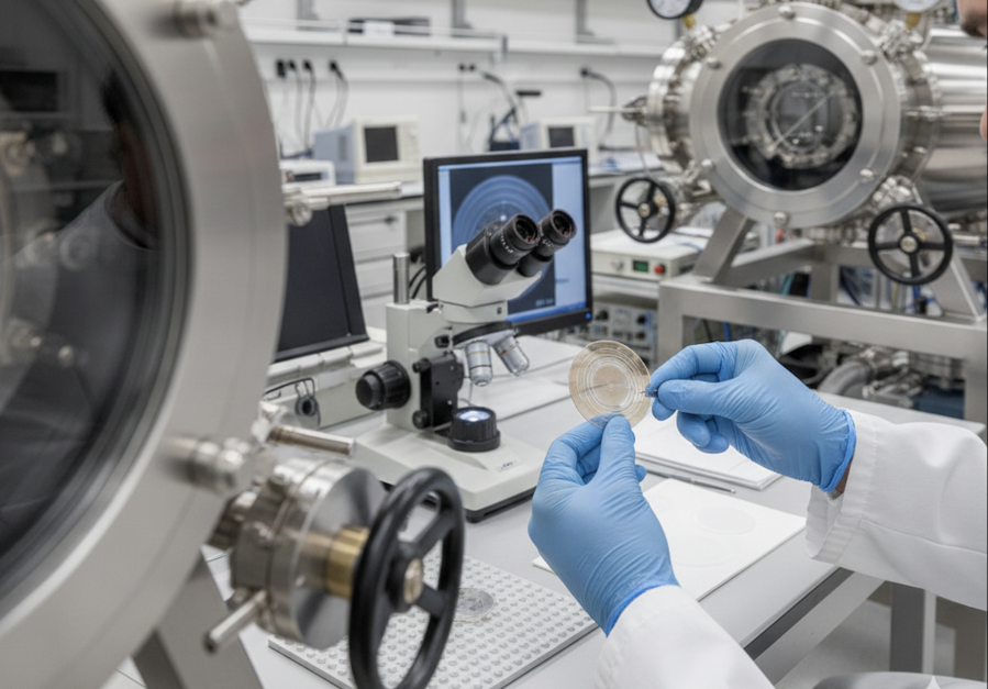
UHV Chamber Surface Treatment Verification
If the Ultra-High Vacuum surface treatment is not done correctly, the 8nm process requirements will not be met as this UHV chamber will fail to manufacture microscopic equipment with precision. This is why, for semiconductor equipment manufacturers and wafer fabs or scientific research institutions, validating the surface treatment after careful metrology is important. Here are some common verification techniques:
- Profilometry for the measurement of surface roughness
- Residual Gas Analysis to check outgassing nature
- Particle monitoring during process qualification
- X-ray photoelectron spectroscopy for surface chemistry analysis
Results from these verification techniques provide quantitative proof if the Ultra-High Vacuum chamber surface treatment meets the 8nm process requirements or not.
Conclusion
As the semiconductor manufacturing industry dives deeper into manufacturing nanoscopic technology nodes, the challenge is increasing to do so with a high level of precision. This is why, UHV chambers’ surface treatment of advanced level is a must for critical success in this field.
For semiconductor equipment manufacturers and wafer fabs, choosing a professional Ultra High Vacuum chamber manufacturer like 'Laiku' who provides advanced modern surface treatment to meet the 8nm manufacturing process. Laiku has a complete solution for your UHV chamber surface treatment with precise control over surface roughness, surface chemistry, electropolishing, plasma cleaning, thermal bake out, and other modern techniques.