In the semiconductor industry, lithography stands as a cornerstone process that directly impacts chip performance and yield. From optical research to semiconductor production, lithography plays an indispensable role in creating the intricate patterns that form modern integrated circuits.
Our company specializes in providing high-precision components and equipment for the semiconductor industry, supporting critical manufacturing processes including lithography.

The Significance of Lithography in Semiconductor Manufacturing
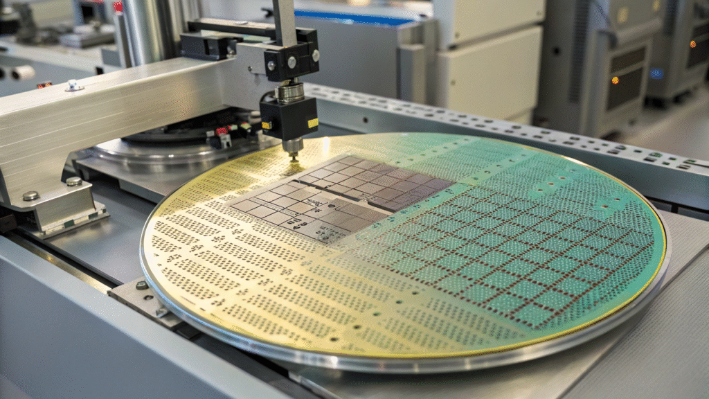
Lithography is the process that transfers circuit patterns onto silicon wafers, essentially "printing" the blueprint for integrated circuits. This critical step determines how many transistors can be packed onto a chip and directly influences performance, power consumption, and cost.
In semiconductor manufacturing, lithography systems must operate in highly controlled environments to ensure the purity and precision required for proper pattern transfer onto silicon wafers.
Core Lithography Processes in Chip Manufacturing
The lithography process involves several precise steps:
- Substrate Preparation - Preparing the silicon wafer surface
- Photoresist Application - Coating the wafer with light-sensitive material
- Exposure - Projecting the circuit pattern through a mask
- Development - Removing exposed or unexposed photoresist
- Etching - Transferring the pattern to underlying layers
- Photoresist Removal - Cleaning the remaining photoresist
Each step requires rigorous control to ensure pattern quality and fidelity, especially as feature sizes continue to shrink in advanced nodes.
Advanced Lithography Technologies
As semiconductor manufacturers push toward smaller transistors and higher densities, lithography technologies have evolved significantly:
- Deep Ultraviolet (DUV) Lithography - Using 193nm wavelength light for current production nodes
- Extreme Ultraviolet (EUV) Lithography - Employing 13.5nm wavelength light for cutting-edge chips
- Multiple Patterning - Techniques that enable features smaller than the wavelength of light used
- Immersion Lithography - Using liquid between the lens and wafer to improve resolution
These advanced methods require ultra-clean environments and precision manufacturing that our vacuum chambers and components are designed to support.
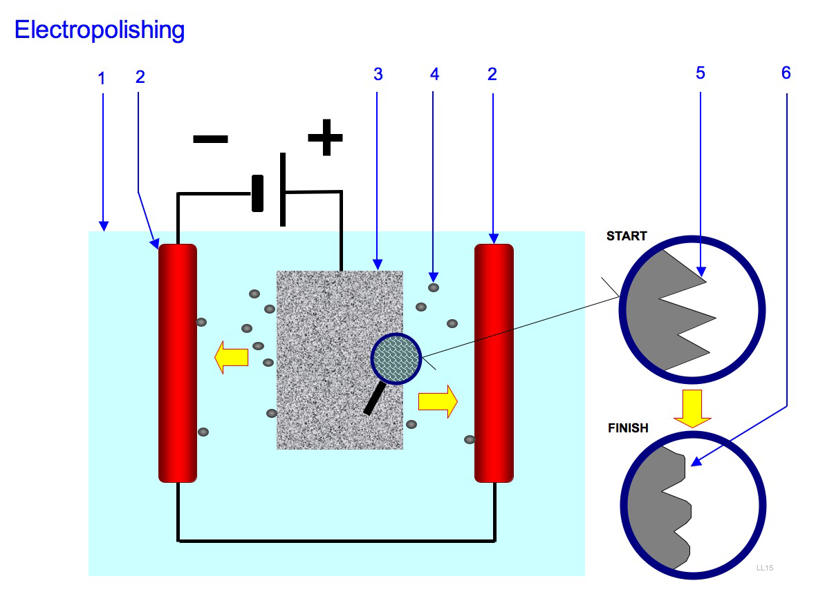
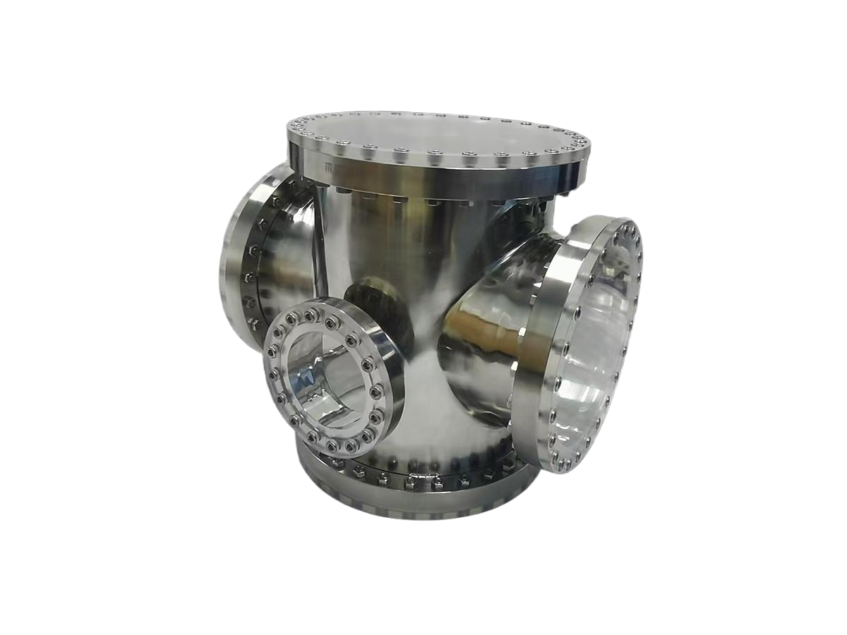
Vacuum Systems in Lithography Equipment
Vacuum technology plays a crucial role in lithography systems, particularly for EUV lithography which must operate in high vacuum conditions. Our specialized vacuum chambers provide the controlled environment essential for:
- Preventing photoresist contamination
- Enabling precise optical path control
- Supporting stable temperature conditions
- Maintaining cleanliness standards required for nanometer-scale features
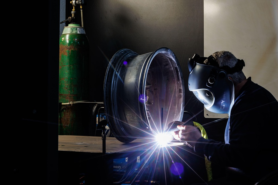
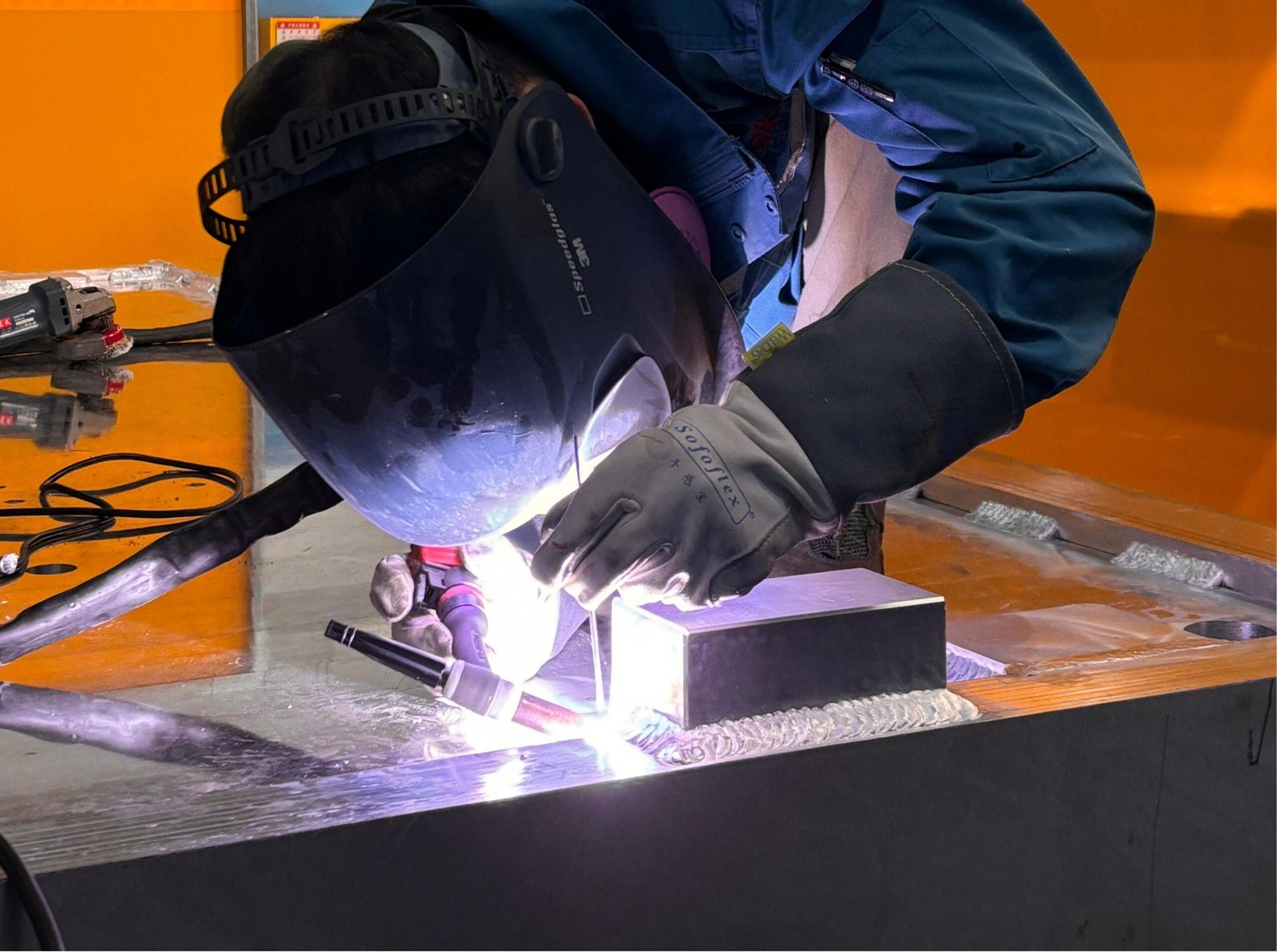
We specialize in creating custom vacuum chambers that meet the stringent requirements of lithography equipment manufacturers, ensuring optimal performance for these complex systems.
Quality Control in Lithography Components
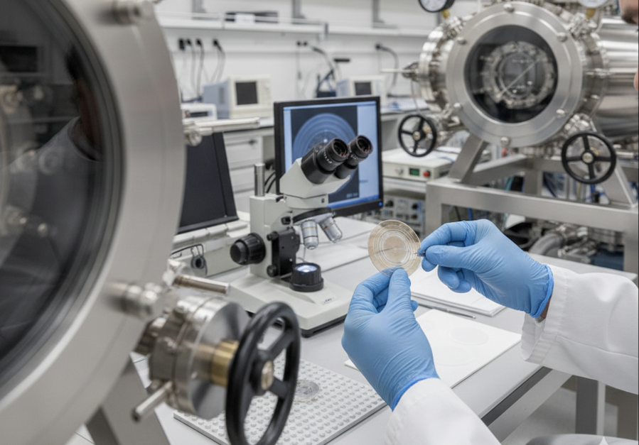
For lithography equipment, component quality directly impacts process precision. Our manufacturing process includes rigorous quality control:
- On-machine inspection during production
- Secondary dimensional inspection using CMM machines with a 4000mm inspection range
- Detailed quality reports for each component
These quality processes ensure our components meet the exacting standards required for lithography equipment in semiconductor manufacturing.
Supporting the Semiconductor Manufacturing Ecosystem
Beyond lithography, our company supports the broader semiconductor manufacturing ecosystem with high-precision components for:
- Deposition processes (PVD, CVD)
- Etching equipment
- Testing and inspection systems
With our expertise in precision manufacturing, surface treatments, and vacuum technology, we provide integrated solutions that address the complex requirements of semiconductor manufacturing.
Conclusion
Lithography remains one of the most challenging and critically important steps in semiconductor chip production. As feature sizes continue to shrink and chip designs grow more complex, the demand for ultra-precise manufacturing and reliable vacuum systems will only increase. Our company is committed to delivering the high-quality components that enable these advanced manufacturing processes, helping our clients maintain technological leadership in the competitive semiconductor market.