
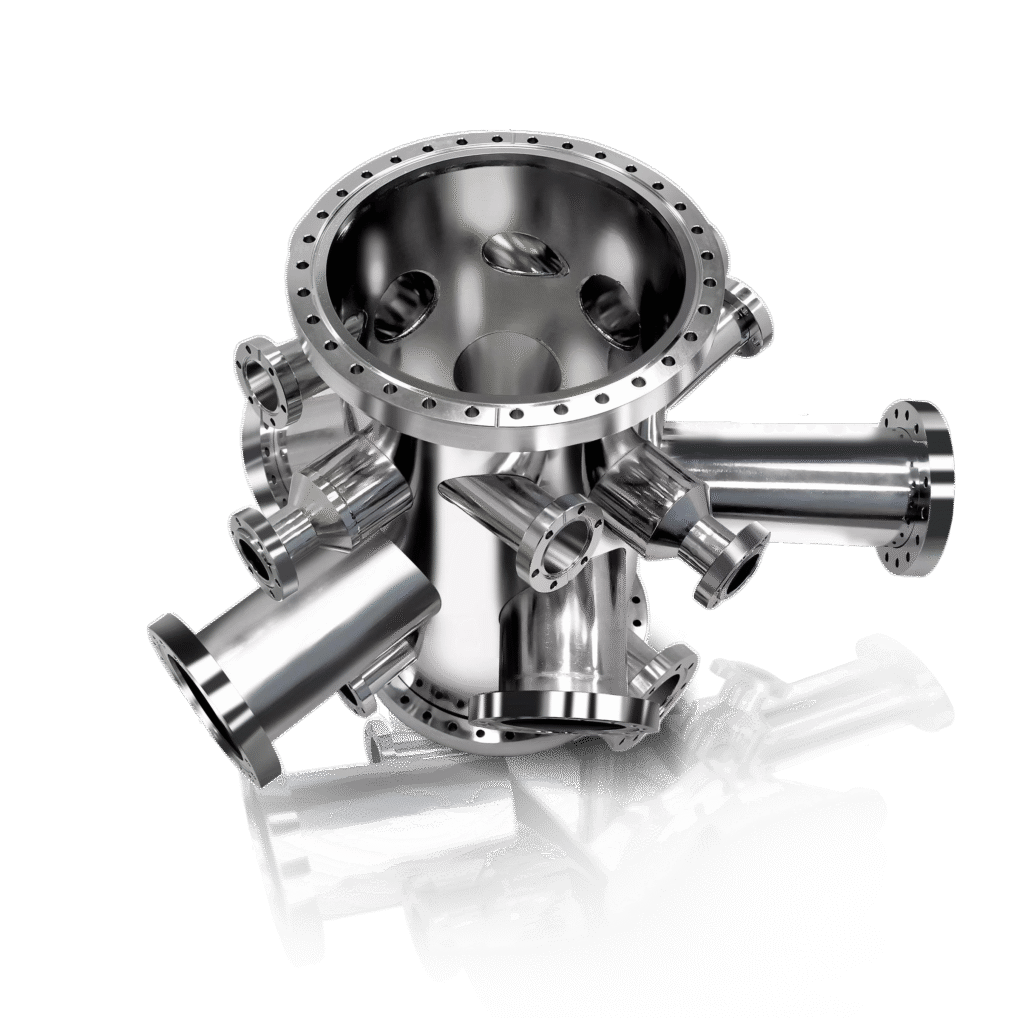
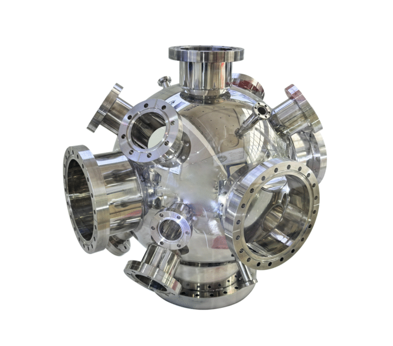
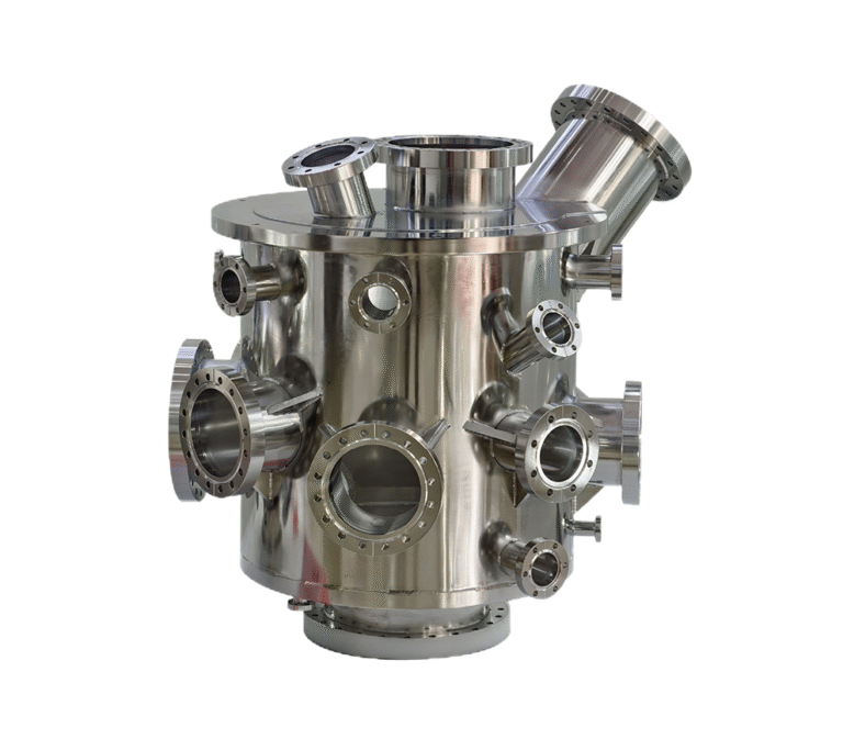
Spherical stainless steel vacuum chamber
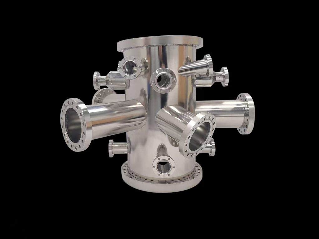
Cylindrical stainless steel vacuum chamber
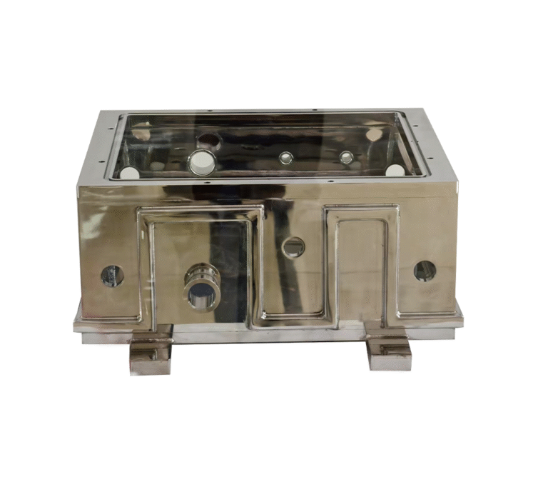
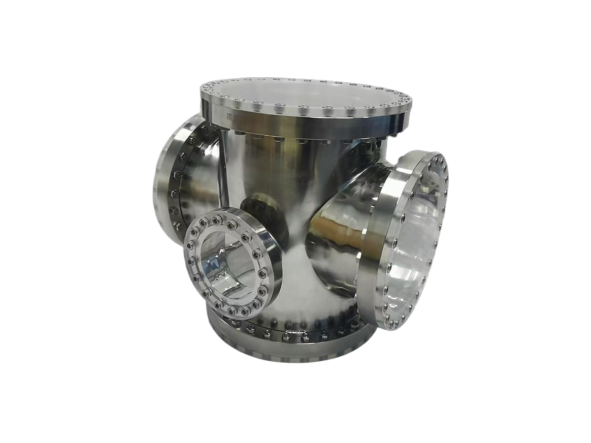
Square stainless steel vacuum chamber
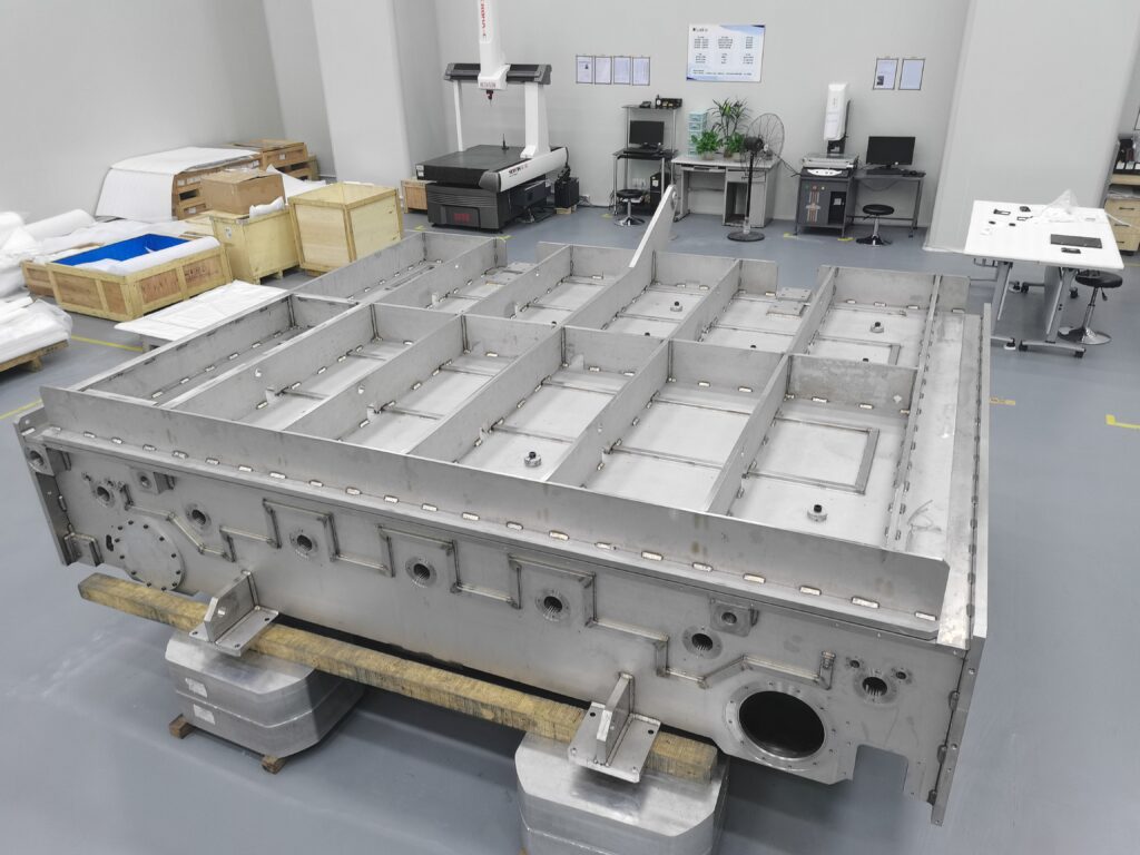
Large stainless steel chamber
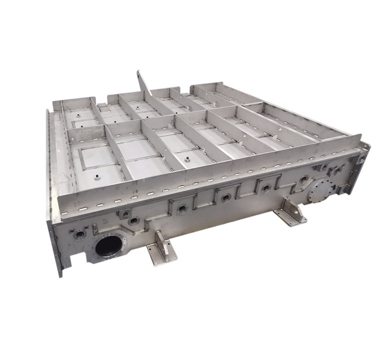
Large aluminum alloy chamber
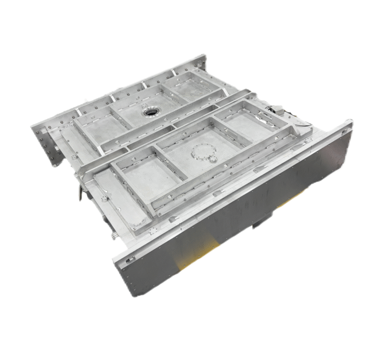
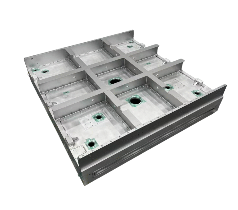
Large aluminum alloy chamber
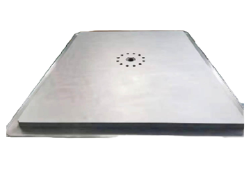
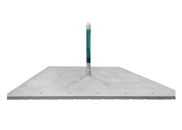
backing plate
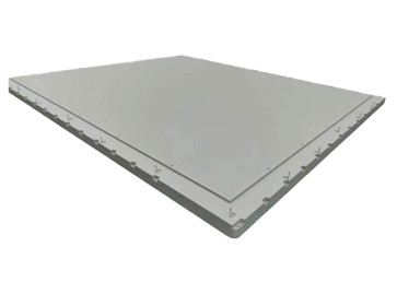
Diffuser
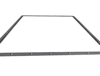
Shadow Frame
Susceptor


How to Choose the Right Welding Supplier: Key Criteria and Company Selection Guide
The selection of a suitable welding supplier cannot be confined to finding the cheapest or lowest price and the quickest
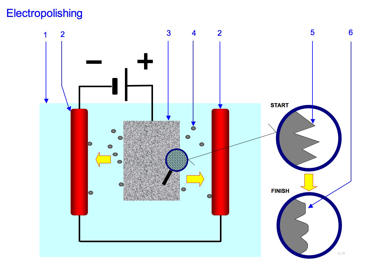
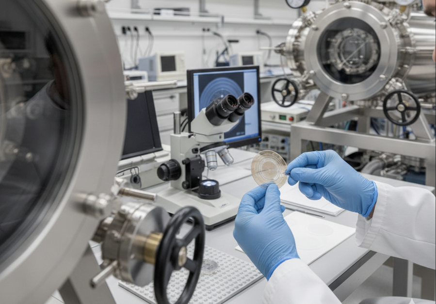
Breakthrough in Ultra-High Vacuum Chamber Surface Treatment: How to Meet 8nm Process Requirements?
How precise can the surface treatment be? – This question is being redefined with semiconductor industry advances toward the 8nm
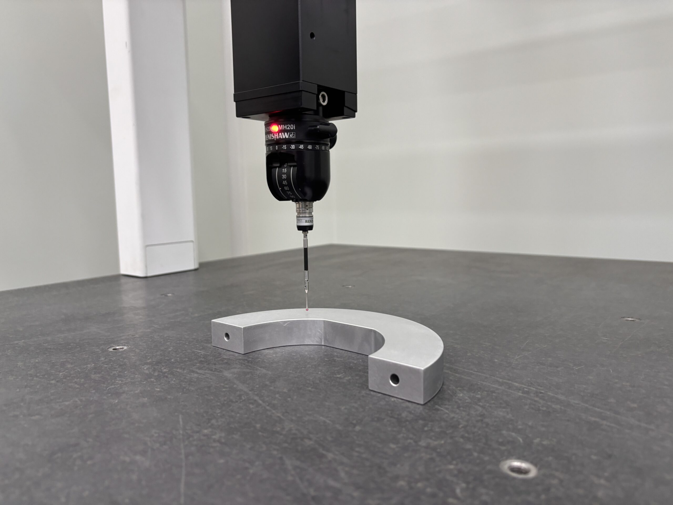
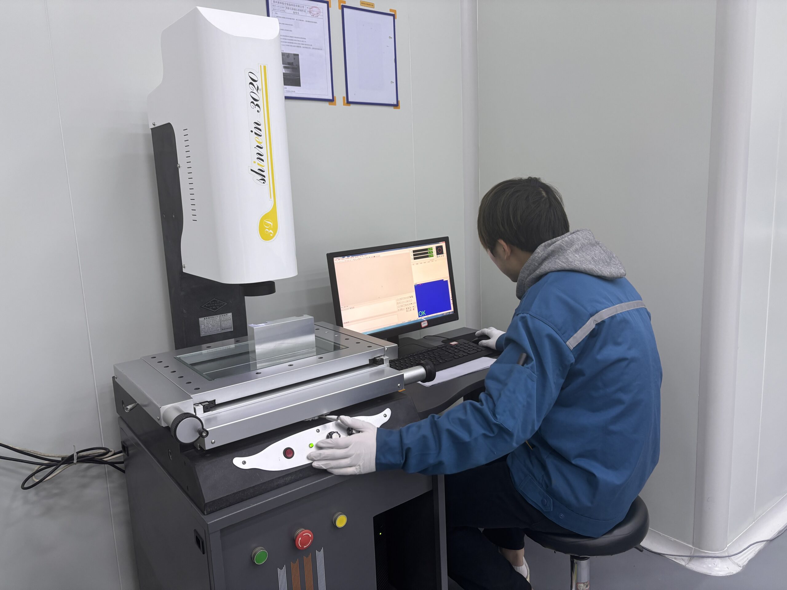
How to Overcome Quality Control Challenges in the Manufacturing of Ultra-High Vacuum Chambers
In Ultra-High Vacuum (UHV) manufacturing, quality control is not a compliance exercise; it is a strategic differentiator. At pressures below
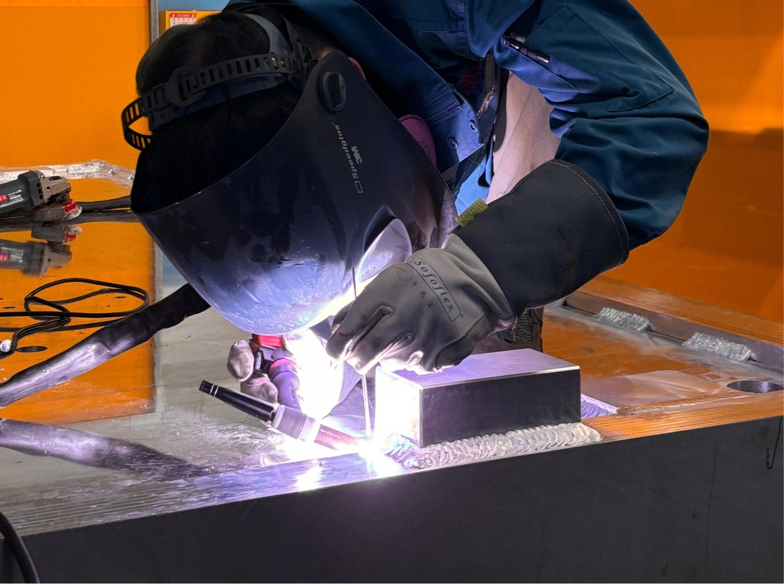
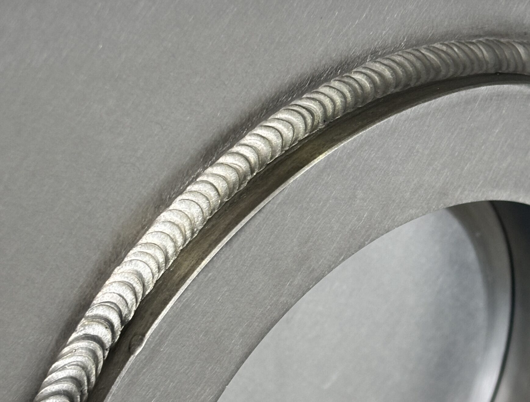
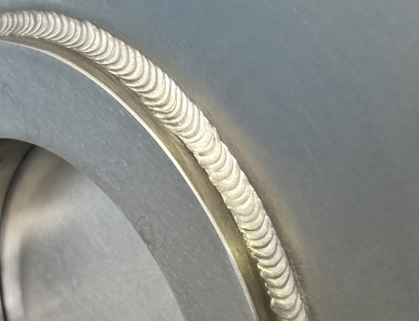
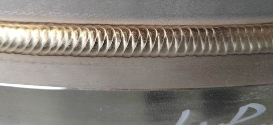
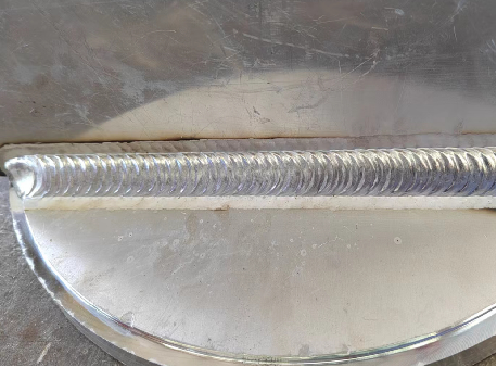
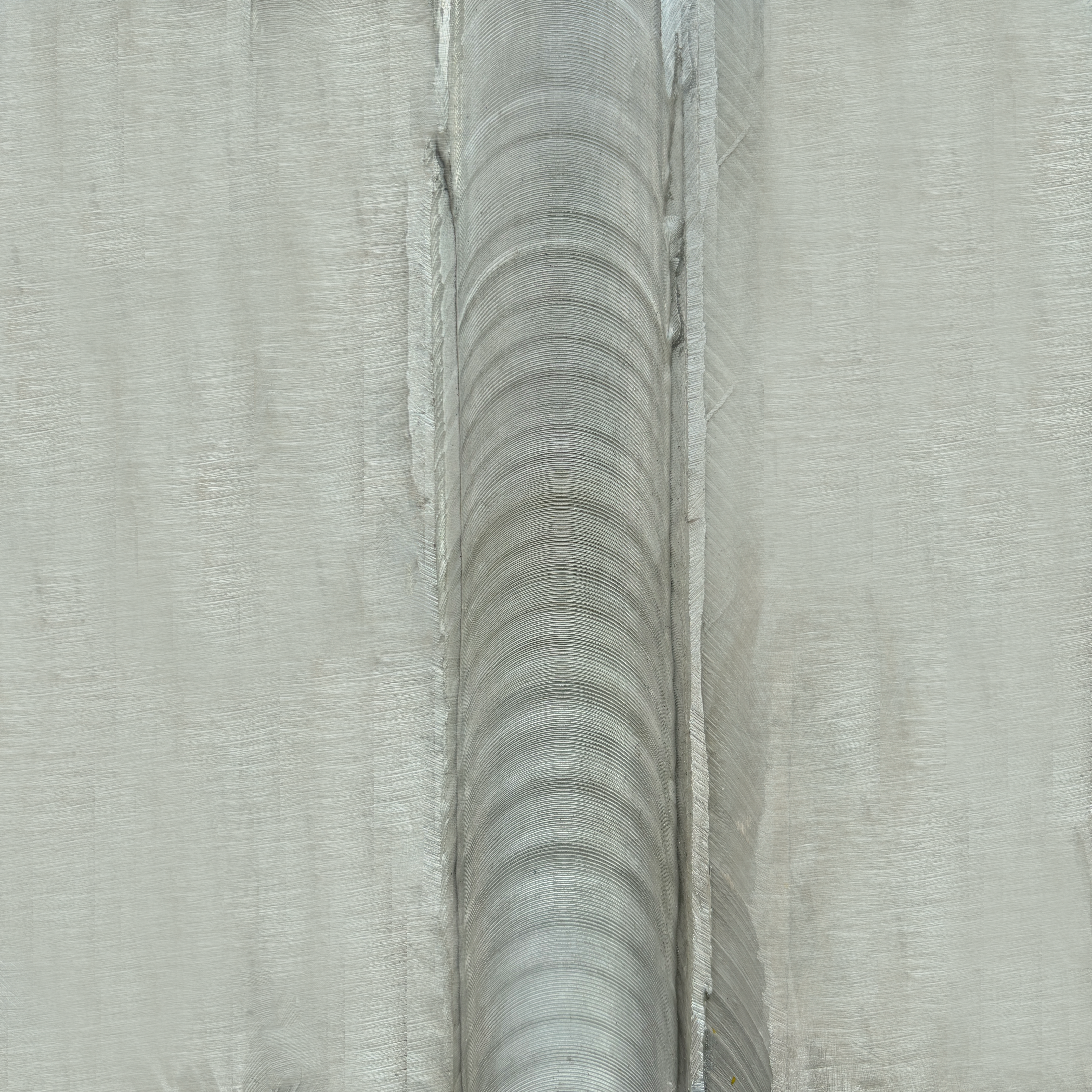
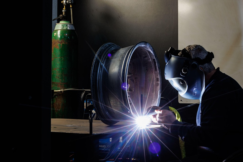
How to Address Welding and Connection Technology Challenges in Ultra-High Vacuum Environments?
Ultra-high vacuum environments create significant challenges for welding and connections. Leaks, contamination, and material failures can compromise system performance and
How to Address Welding and Connection Technology Challenges in Ultra-High Vacuum Environments?
The demanding world of ultra-high vacuum systems presents persistent welding and connection challenges that compromise system integrity. Manufacturers face leakage,
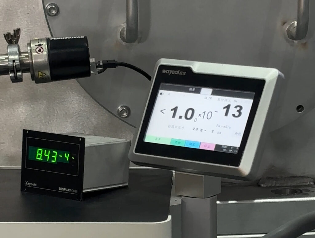
Vacuum System Leak Detection Technology and Quality Assurance System
Vacuum leaks can devastate production lines, waste materials, and create costly delays. Finding these invisible problems quickly can mean the
Spherical stainless steel vacuum chamber
Cylindrical stainless steel vacuum chamber
Square stainless steel vacuum chamber
Large stainless steel chamber
Large aluminum alloy chamber
Large aluminum alloy chamber
backing plate
Diffuser
Shadow Frame
Susceptor
How to Choose the Right Welding Supplier: Key Criteria and Company Selection Guide
The selection of a suitable welding supplier cannot be confined to finding the cheapest or lowest price and the quickest
Breakthrough in Ultra-High Vacuum Chamber Surface Treatment: How to Meet 8nm Process Requirements?
How precise can the surface treatment be? – This question is being redefined with semiconductor industry advances toward the 8nm
How to Overcome Quality Control Challenges in the Manufacturing of Ultra-High Vacuum Chambers
In Ultra-High Vacuum (UHV) manufacturing, quality control is not a compliance exercise; it is a strategic differentiator. At pressures below
How to Address Welding and Connection Technology Challenges in Ultra-High Vacuum Environments?
Ultra-high vacuum environments create significant challenges for welding and connections. Leaks, contamination, and material failures can compromise system performance and
How to Address Welding and Connection Technology Challenges in Ultra-High Vacuum Environments?
The demanding world of ultra-high vacuum systems presents persistent welding and connection challenges that compromise system integrity. Manufacturers face leakage,
Vacuum System Leak Detection Technology and Quality Assurance System
Vacuum leaks can devastate production lines, waste materials, and create costly delays. Finding these invisible problems quickly can mean the