Ever tampered with a vacuum chamber leak during a critical semiconductor process? It's frustrating – one minor flaw can derail an entire batch. At SZLK SEMI, we've built customized chambers for clients like leading equipment firms, and know firsthand: designing for 10^−6 Torr pressures (that's near-perfect vacuum) demands precision. See, in high-tech devices like lithography tools, tiny gas molecules interfere with plasma etching or deposition, causing yield losses over 15% in some foundries. That's why mastering ultimate vacuum isn't just engineering; it's business-critical. Let's break down the core principles to keep your systems robust and efficient.
Understanding Ultimate Vacuum in Semiconductor Context
Ultimate vacuum refers to pressures below 10^−6 Torr, where air molecules number fewer than a few billion per cubic centimeter. Why care? In semiconductor fabrication, even residual gases alter chemical reactions in processes like RF sputtering. For instance, moisture traces can oxidize silicon wafers, creating defects that cost millions annually. Practical tip: aim for UHV (ultra-high vacuum) standards as defined by SEMI's F51-0300, not just rough vacuums – it ensures repeatability in mass production environments.
Key Design Principles for Robust Vacuum Attainment
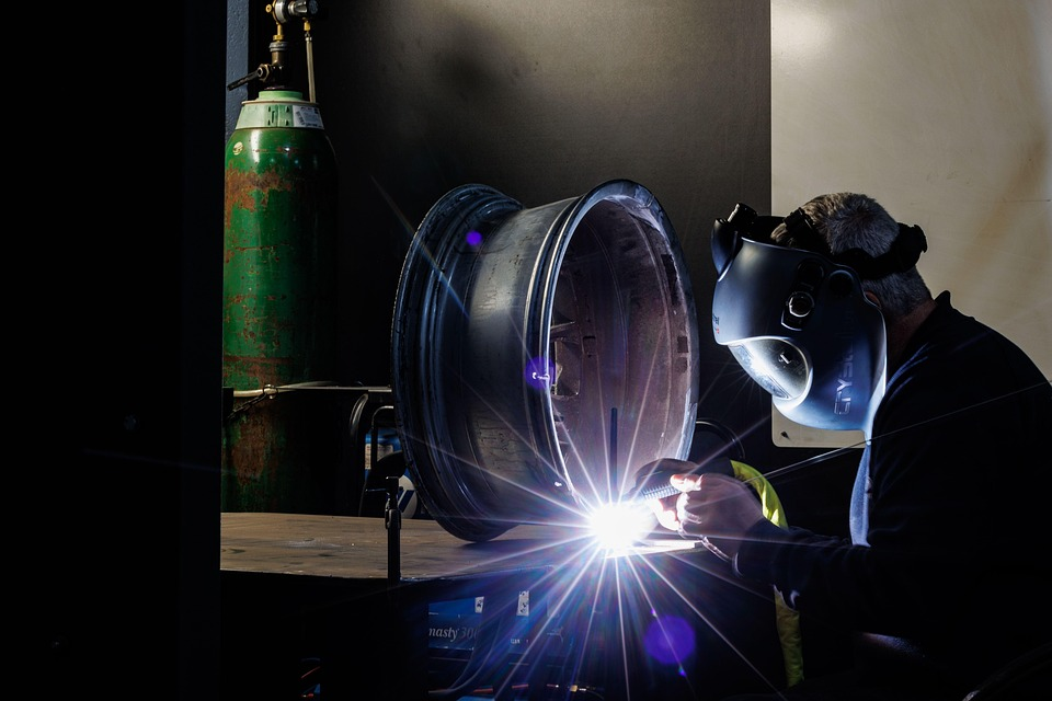
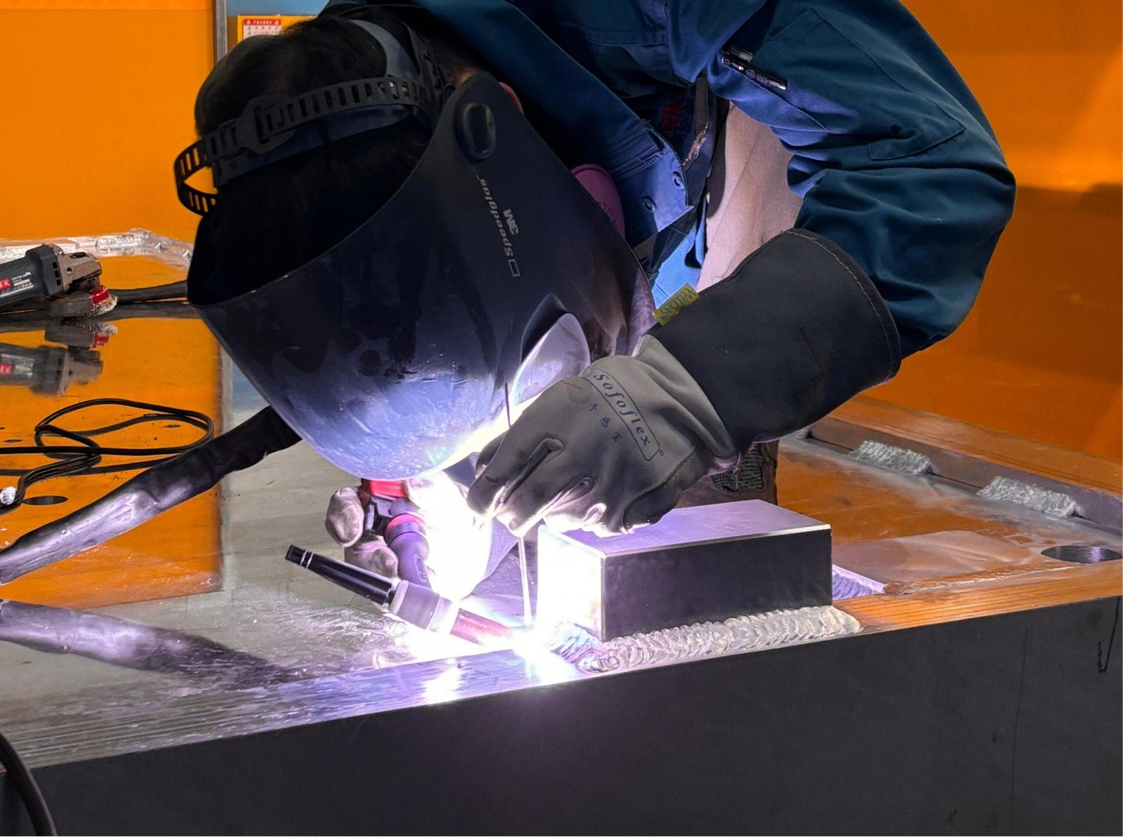
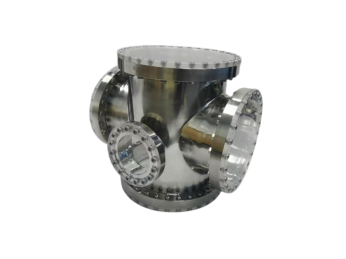
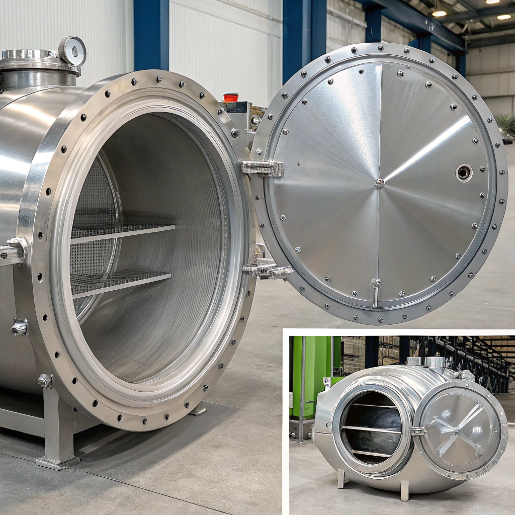
First off, forget one-size-fits-all. Chambers must be airtight: focus on materials and geometry. Choose low-outgassing materials like 316L stainless steel; we once customized a chamber with electropolished interiors for a crystal growth tool, reducing particulates by 30%. Geometry matters too – smoothed surfaces prevent turbulence that traps gases. Also, balance pump integration: turbo pumps combined with cryogenic systems pump gases faster. Remember, small errors amplify; a minute leak near bearing seals can push recoveries to hours. Test rigorously with helium-based detectors before deployment.
Material Choices and Fabrication Tips
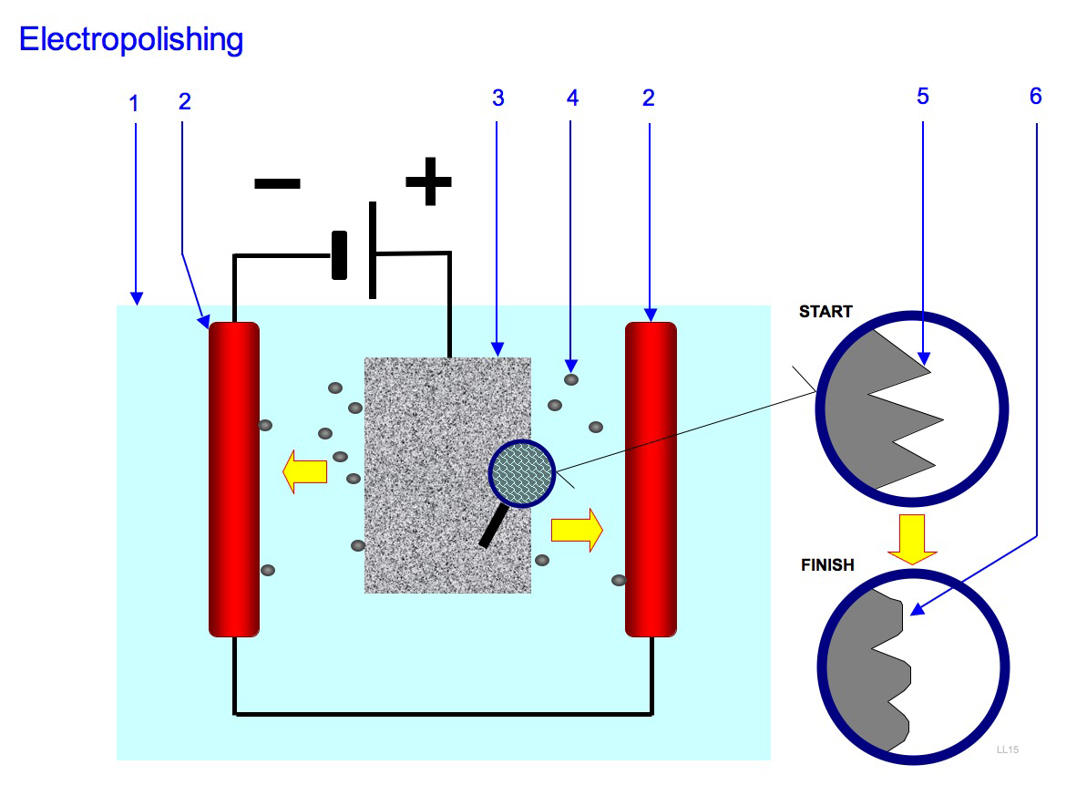
Not all metals behave the same under vacuum. Aluminium often outgasses volatile ions, risking contamination. Instead, grade-2 titanium or specialized coatings (like aluminum oxide) offer corrosion resistance while minimizing adsorption – a win for high-purity deposition chambers. At SZLK SEMI, we build chambers using CNC machining and laser welding for near-seamless joints. This precision avoids micro-fractures that plague mass-produced units. Case study: one client saw 50% longer maintenance intervals after switching to our bespoke design. If you're procuring, demand material certifications to avoid surprises at scale– shop smarter!
Implementing in Semiconductor-Specific Applications
Now, apply this to real devices. In ion implants, customize chamber dimensions to match beam angles – a misfit stresses internal components. Leverage bake-out processes at 150°C for 48 hours to desorb gases; we've helped firms like innovators cut pump-down times by 20%. Also, monitor with gauges strategically: place pressure sensors near high-stress zones. Future-proofing: as EUV lithography advances, chambers need coatings that resist hydrogen embrittlement. In short, tailor designs for the task – that's how top labs achieve reliably low pressures weekly.
Designing vacuum chambers for ultimate levels isn't magic; it's meticulous mechanics. By prioritizing material quality, leak-proof fabrication, and custom fits, your semiconductor tools will operate smoother – saving costs and downtime. Got unique challenges? Share them with SZLK SEMI's team; we engineer solutions that make vacuums work harder. Because in high-stakes industries, the air shouldn't.