The semiconductor industry faces unprecedented pressure to advance node technology while controlling costs. Traditional vacuum chambers fail to meet the extreme precision demands of sub-3nm processes, resulting in yield issues and manufacturing bottlenecks.
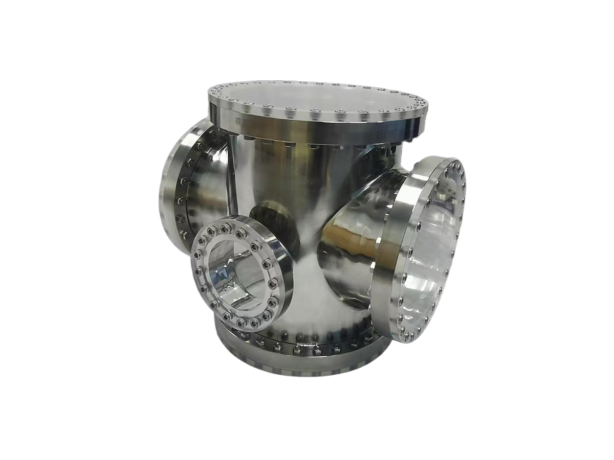
Advanced process semiconductor vacuum chambers require extraordinary precision, contamination control, and material purity beyond conventional manufacturing capabilities. These specialized components enable critical processes like extreme ultraviolet lithography, atomic layer deposition, and high-aspect-ratio etching essential for next-generation chip production.
As semiconductor manufacturers push toward smaller node sizes and more complex architectures, the demands placed on vacuum chamber technology have increased exponentially. Understanding these challenges and emerging opportunities is essential for anyone involved in the semiconductor equipment supply chain.
What Makes Vacuum Chambers Critical for Advanced Process Semiconductor Equipment?
Semiconductor manufacturers struggle with contamination issues that cause nanoscale defects in advanced processes. Even single-digit parts-per-billion impurities can dramatically reduce yield rates, costing millions in wasted production.
Modern semiconductor vacuum chambers provide the ultra-pure environments essential for advanced processes, controlling particle counts, moisture levels, and oxygen concentration to unprecedented levels. These chambers enable critical technologies like EUV lithography and atomic layer deposition that form the foundation of sub-3nm process nodes.

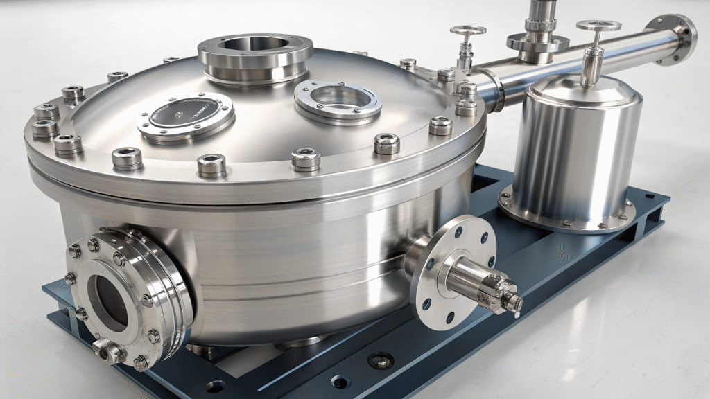
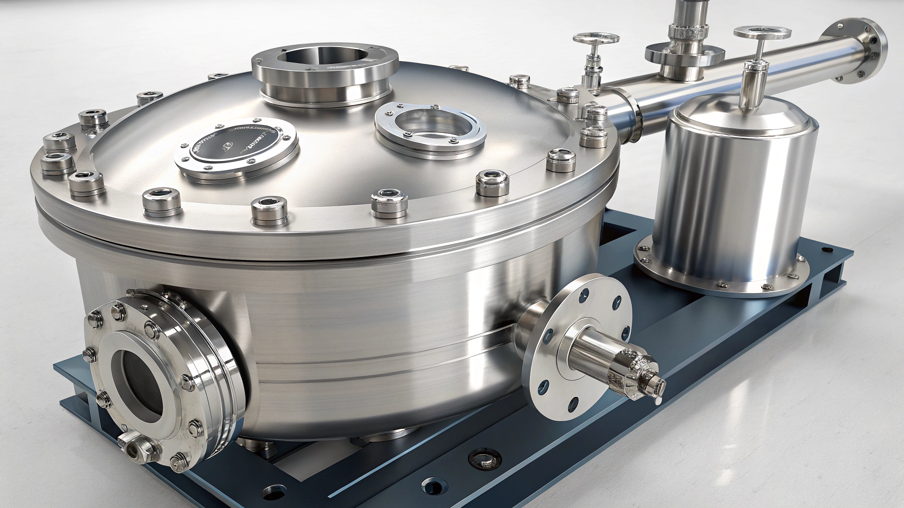
The evolution of semiconductor manufacturing technology has placed extraordinary demands on vacuum chamber design and performance. While vacuum technology has long been a cornerstone of semiconductor fabrication, advanced process nodes have transformed what was once primarily a matter of pressure control into a multidimensional engineering challenge.
The most advanced semiconductor processes now operate at scales where quantum effects become significant and single-atom deviations can impact device performance. This reality necessitates vacuum environments that maintain not just low pressures but extraordinarily precise control of residual gases, particles, temperature, electromagnetic fields, and vibration.
Our experience designing chambers for leading semiconductor equipment manufacturers has shown that advanced process vacuum chambers typically need to maintain base pressures in the 10⁻⁹ to 10⁻¹¹ Torr range while handling substantial gas loads during processes. Achieving these conditions requires sophisticated pumping arrangements often combining turbomolecular pumps, cryopumps, and specialized getter materials strategically positioned throughout the chamber system.
For extreme ultraviolet (EUV) lithography applications, chambers must maintain exceptional cleanliness while handling the unique challenges of EUV radiation, including secondary electron generation, carbon contamination control, and hydrogen management. Our chamber designs for these applications incorporate specialized coatings that minimize secondary electron emission while providing resistance to radiation damage and maintaining vacuum integrity through thousands of exposure cycles.
Advanced etch and deposition processes present different but equally demanding challenges, including the need to handle highly reactive gases and plasmas while maintaining precise temperature control across complex chamber geometries. We address these requirements through carefully engineered gas delivery systems, optimized RF power coupling designs, and sophisticated thermal management solutions that maintain component temperatures within ±0.5°C even under varying process conditions.
What Material Innovations Are Enabling Next-Generation Semiconductor Vacuum Chambers?
Traditional materials used in vacuum chambers release unacceptable levels of contaminants in advanced semiconductor processes. Standard manufacturing approaches simply cannot achieve the material purity necessary for sub-3nm nodes.
Next-generation semiconductor vacuum chambers utilize specialized high-purity materials including custom stainless steel alloys, exotic metals like tantalum and niobium, and advanced ceramic components. These materials undergo extraordinary purification processes and surface treatments to ensure compatibility with the most demanding semiconductor processes.
Material science advancements have revolutionized vacuum chamber technology for semiconductor applications, enabling process capabilities that were previously impossible. The materials used in advanced semiconductor vacuum chambers must satisfy an extremely challenging set of requirements including ultra-high purity, minimal outgassing, excellent dimensional stability, and resistance to process chemicals.
For chamber structural components, we've developed proprietary processing methods for specialized stainless steel alloys including 316L and 304L that reduce gas content and metallic impurities far below industry-standard levels. These advanced materials undergo multiple refining steps including vacuum arc remelting and specialized heat treatments to achieve exceptionally consistent microstructures with minimal inclusion content. The result is base materials with significantly reduced potential for outgassing or particle generation during thermal cycling.
For components directly exposed to plasma processes or aggressive chemistry, we implement specialized materials including high-purity aluminum alloys with carefully controlled composition. These materials undergo proprietary surface treatments that create exceptionally stable oxide layers, minimizing both chemical interaction with process gases and particle generation during operational cycles. For particularly demanding applications, we employ exotic materials including molybdenum, tantalum, and specialized ceramics such as aluminum nitride or sapphire.
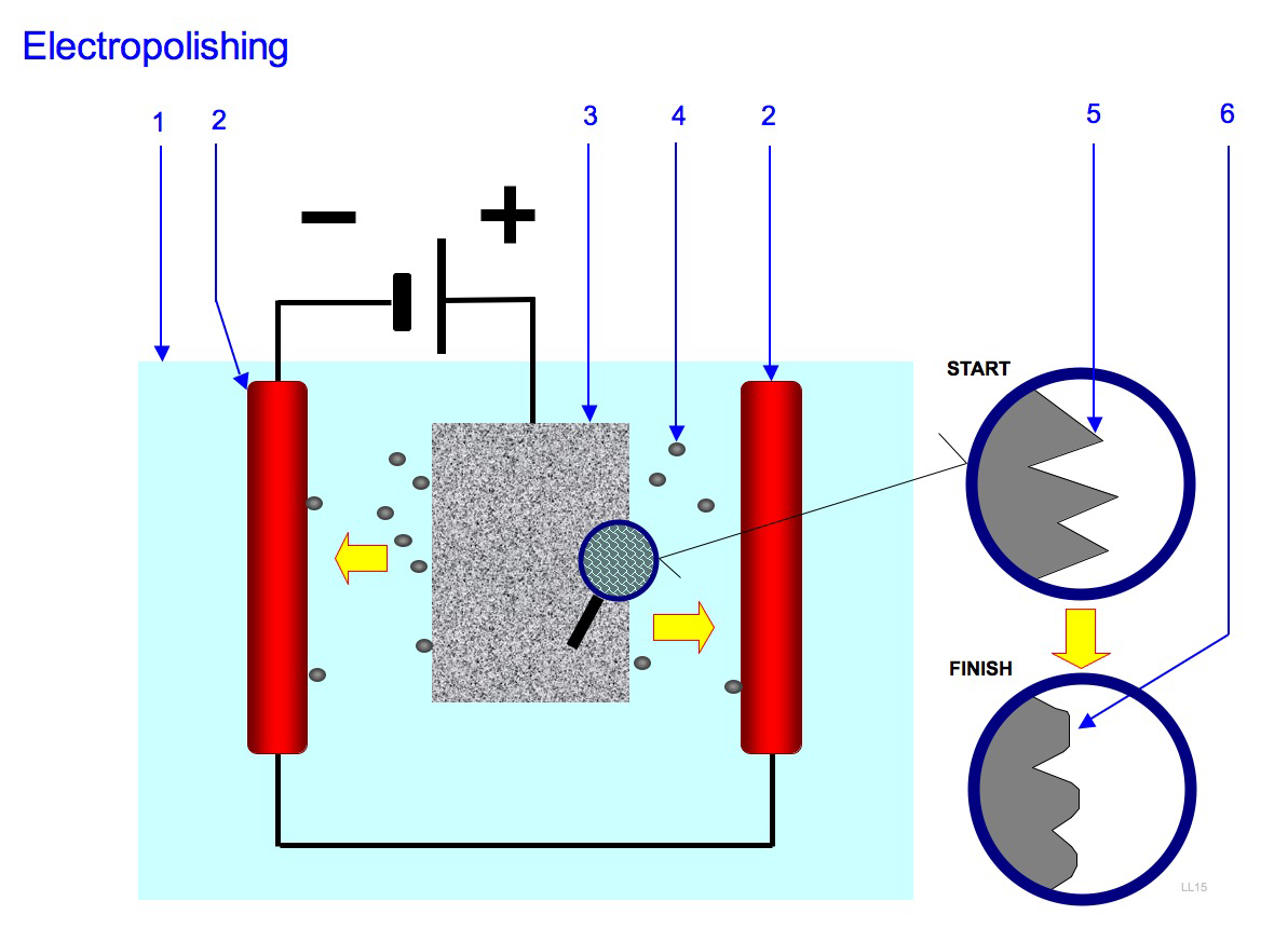
Surface finishing technologies have advanced dramatically to support semiconductor vacuum requirements. Our chambers utilize multi-stage surface preparation protocols culminating in electropolishing processes specifically developed for semiconductor applications. These processes achieve surface roughness values below 0.2 μm Ra while removing potential contamination sources embedded in the material surface. For critical components, we implement additional surface passivation treatments that further enhance stability under process conditions.
Sealing technology represents another area of significant material innovation. Traditional elastomeric seals cannot meet the stringent requirements of advanced semiconductor processes due to permeation and outgassing concerns. We've developed specialized all-metal sealing solutions using carefully formulated alloys that provide reliable sealing performance while minimizing potential contamination. These sealing systems maintain integrity through hundreds of thermal cycles while contributing virtually zero organic contaminants to the process environment.
Perhaps most importantly, our material selections incorporate comprehensive consideration of long-term stability under process conditions. Materials that appear suitable based on initial properties may prove problematic after exposure to process chemistry or energy inputs. Our testing protocols include accelerated aging under simulated process conditions to verify material performance over the expected chamber lifetime.
How Are Precision Manufacturing Techniques Evolving for Semiconductor Vacuum Chambers?
Conventional manufacturing techniques cannot achieve the dimensional accuracy required for advanced semiconductor processes. Chamber misalignment measured in micrometers can disrupt critical process steps and damage expensive wafers.
Semiconductor vacuum chamber manufacturing now employs advanced techniques including 5-axis machining with in-process measurement, electron beam welding in controlled environments, and advanced metrology using coordinate measuring machines accurate to submicron levels. These processes ensure chambers meet the extreme precision requirements of advanced node fabrication.
The manufacturing methodologies for semiconductor vacuum chambers have undergone a radical transformation to meet the precision requirements of advanced process nodes. What was once primarily focused on achieving good vacuum performance has evolved into an exacting discipline requiring unprecedented control of dimensions, surface conditions, and material properties.
Our manufacturing facilities implement a comprehensive approach beginning with environmental control throughout the production process. Critical machining operations occur in temperature-controlled environments maintained at 20°C ±0.5°C to minimize thermal expansion effects during precision operations. For components with tolerances below 10 micrometers, we employ stabilization periods between manufacturing steps to allow material stress relaxation and ensure dimensional stability in the final product.
Advanced multi-axis machining centers with thermal compensation systems form the foundation of our manufacturing capabilities. These systems incorporate in-process measurement using contact and optical methods to verify critical dimensions during machining operations. This approach eliminates the dimensional variations that can occur when parts are removed and reinstalled for inspection, ensuring exceptional consistency across complex geometries.
Joining processes for advanced semiconductor chambers have evolved well beyond traditional welding techniques. We employ specialized electron beam welding in controlled vacuum environments to create joints with minimal heat-affected zones and exceptional purity. For particularly critical applications, we utilize proprietary solid-state joining methods that create molecular-level bonds without introducing the thermal stresses associated with fusion welding.
Surface finishing for semiconductor chambers involves multiple specialized processes tailored to specific component requirements. Our approach begins with precision machining to establish base geometry, followed by carefully controlled mechanical processing to achieve preliminary surface finish targets. Components then undergo chemical processing and electropolishing in cleanroom environments using ultrapure chemicals and deionized water with resistivity exceeding 18 megohm-cm.
Quality verification employs advanced metrology systems including coordinate measuring machines with accuracy to 0.5 micrometers and optical scanning technologies capable of capturing complete component geometries for comparison against CAD models. These systems operate in temperature-controlled environments and utilize advanced software to compensate for remaining environmental variables.
Cleanliness verification represents the final critical step in our manufacturing process. Components undergo residual gas analysis using mass spectrometry to verify outgassing characteristics, particle testing using specialized optical scanning systems, and materials analysis to confirm surface composition. These comprehensive verification steps ensure that chambers will meet the extraordinary cleanliness requirements of advanced semiconductor processes.
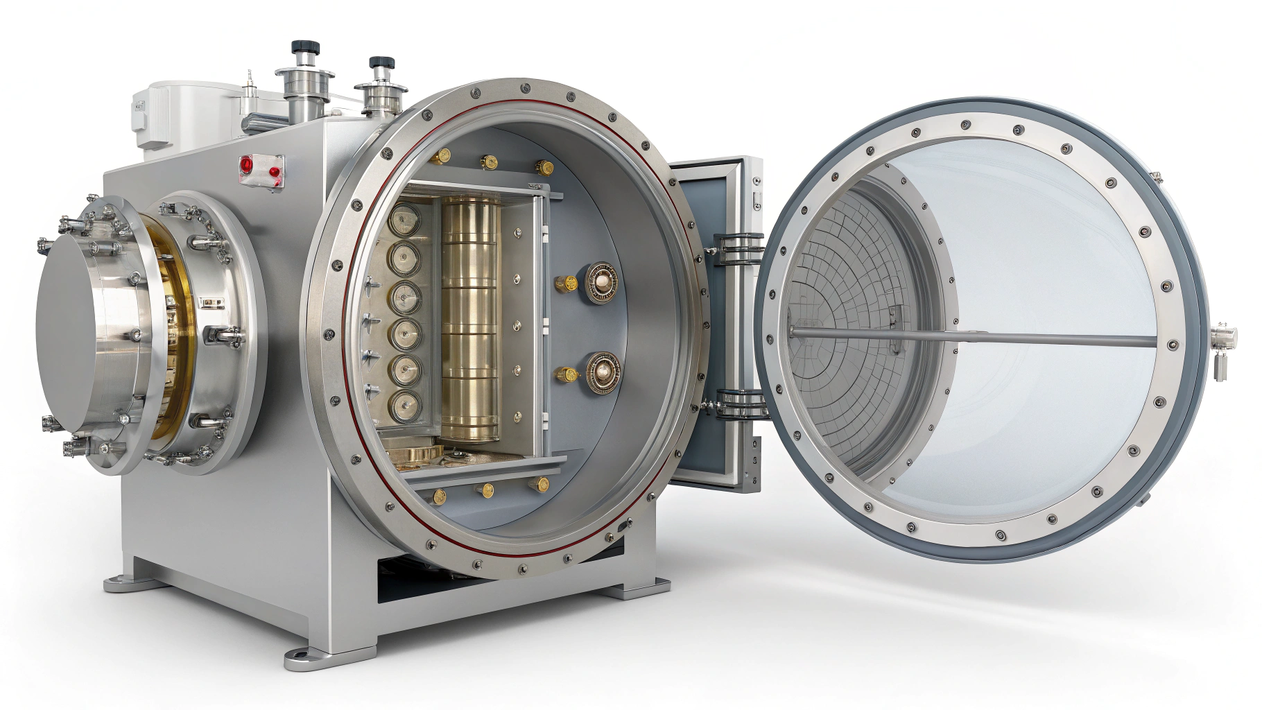
What Integration Challenges Exist for Vacuum Chambers in Complex Semiconductor Tools?
Equipment engineers struggle with integrating vacuum chambers into increasingly complex semiconductor tool architectures. Compatibility issues between subsystems lead to costly redesigns and delayed tool qualifications, impacting production schedules.
Semiconductor vacuum chamber design now requires sophisticated integration approaches including standardized interfaces, modular architectures, and comprehensive simulation of system-level performance. These advanced design methodologies ensure seamless integration with adjacent subsystems including wafer handling mechanisms, power delivery systems, and process gas distribution.
The integration of vacuum chambers into modern semiconductor equipment presents extraordinary challenges that extend far beyond simple mechanical fit. Today's advanced process tools represent some of the most complex machines ever created, combining precision mechanics, sophisticated electronics, advanced optics, and reactive chemistry within tightly constrained spaces.
Our approach to vacuum chamber integration begins in the earliest design phases with comprehensive modeling of the complete tool environment. We employ sophisticated CAD systems with enhanced capabilities for tolerance stack analysis, thermal expansion modeling, and simulation of dynamic interactions between components. This approach identifies potential interference issues, access limitations, and maintenance challenges before physical prototyping begins.
Interface standardization represents a critical element of our integration strategy. We've developed proprietary flange designs and connection systems specifically optimized for semiconductor applications. These systems incorporate features that ensure precise alignment during assembly while accommodating the inevitable dimensional variations that occur during manufacturing. For critical interfaces, we implement kinematic mounting principles that provide consistent positioning through multiple assembly cycles.
Service access represents another significant integration challenge, particularly as tool architectures become increasingly dense. Our designs incorporate thoughtful consideration of maintenance requirements, with strategic placement of access ports, removable sections, and quick-disconnect utilities. Where possible, we implement modular designs that allow removal of specific sections for service without disturbing adjacent systems that may require extensive recalibration.
Thermal management across integrated systems presents particular challenges in semiconductor equipment. Our vacuum chambers incorporate sophisticated thermal isolation features to prevent heat transfer between components operating at different temperatures. These designs include specialized low-conductivity mounting systems, radiation shields, and strategic placement of active cooling elements. For systems with particularly demanding thermal requirements, we implement advanced control systems that actively manage thermal gradients across multiple subsystems.
Electrical and signal integration has become increasingly complex as semiconductor processes incorporate more sophisticated sensing and control systems. Our chamber designs include carefully engineered feedthrough systems that maintain vacuum integrity while providing the necessary electrical connections. These systems incorporate EMI/RFI shielding where appropriate and utilize specialized materials to minimize potential contamination from electrical components.
Perhaps most importantly, our integration approach includes comprehensive consideration of the entire tool lifecycle from initial installation through eventual decommissioning. We design chambers with features that facilitate initial alignment and qualification, incorporate provisions for potential future upgrades, and ensure that worn components can be replaced without requiring complete system rebuilds.
How Will Future Technology Nodes Impact Vacuum Chamber Requirements?
Semiconductor manufacturers preparing for 2nm processes and beyond face extraordinary challenges in vacuum technology. Current chamber designs will not support the extreme precision and purity requirements of future nodes, potentially limiting industry advancement.
Next-generation semiconductor processes will require vacuum chambers with unprecedented performance including sub-angstrom surface roughness, virtually zero particulate generation, and extraordinary dimensional stability. These advances will enable critical technologies for future computing applications including quantum computing, advanced AI processors, and ultra-high-density memory.
The relentless progression of semiconductor technology toward smaller feature sizes and more complex device architectures will continue to transform vacuum chamber requirements. As the industry moves toward 2nm processes and beyond, several key trends will shape the evolution of vacuum chamber technology.
Process purity requirements will become even more stringent as device features approach atomic dimensions. Future vacuum chambers will likely incorporate advanced in-situ monitoring capabilities including residual gas analyzers and particle detection systems integrated directly into the chamber design. These systems will provide real-time feedback for process control and early detection of potential contamination sources. We're currently developing next-generation chamber materials with impurity levels controlled to parts-per-trillion levels and surface finishes approaching atomic smoothness.
Dimensional stability requirements will increase dramatically for future process nodes. Chambers for advanced lithography applications will need to maintain positioning accuracy measured in nanometers over extended periods while handling substantial thermal loads. These requirements will drive increased use of exotic materials with exceptional stability characteristics, including specialized ceramics, metal matrix composites, and potentially single-crystal components for the most critical applications.
Energy management within vacuum chambers will become increasingly sophisticated as process power densities continue to rise. Future chamber designs will incorporate advanced cooling solutions including microfluidic channels directly integrated into structural components, specialized high-conductivity interfaces, and potentially even phase-change cooling systems for managing extreme heat loads in localized areas.
The trend toward larger wafer sizes presents additional challenges for vacuum chamber technology. As the industry eventually transitions to 450mm wafers, chamber dimensions will increase substantially while tolerance requirements become even more demanding. This combination will necessitate fundamental innovations in manufacturing techniques, material properties, and structural design approaches.
Process integration will continue to evolve, with more process steps occurring within unified vacuum environments to minimize potential contamination from atmospheric exposure. This trend will drive development of increasingly complex multi-chamber systems with sophisticated wafer handling mechanisms operating entirely under vacuum. Our development roadmap includes advanced concepts for module-to-module vacuum interfaces that maintain continuity of the controlled environment while allowing for independent service of individual process modules.
Perhaps most importantly, sustainability considerations will increasingly influence vacuum chamber design. Future systems will need to balance performance requirements against energy consumption, material usage, and end-of-life recycling considerations. We're exploring designs that significantly reduce the mass of chamber components while maintaining necessary performance characteristics, along with material selections that facilitate eventual recycling of components.
Conclusion
Advanced process semiconductor vacuum chambers represent critical enabling technology for continued advancement of the semiconductor industry. By addressing the unique challenges of material purity, precision manufacturing, contamination control, and system integration, specialized vacuum chamber manufacturers play an essential role in facilitating the next generation of semiconductor technology development.