
Have you ever wondered why semiconductor manufacturing requires such precise environments? I've seen firsthand how even the smallest contamination can ruin an entire batch of expensive silicon wafers. Vacuum technology is the unsung hero behind modern electronics.
Semiconductor manufacturing demands extremely high vacuum conditions, particularly in photolithography, etching, and thin film deposition processes. High-quality vacuum systems effectively prevent particle contamination and significantly improve production yields.
Let me dive deeper into the specific vacuum requirements that make our advanced chips possible.
Why is vacuum so critical for semiconductor processes?
Pain point: Manufacturing microchips with billions of transistors requires absolute precision - any contamination can destroy entire production batches worth millions of dollars.
Vacuum systems eliminate particulate and molecular contamination from the air, ensuring the purity of the production environment essential for high-end components like microchips. In semiconductor fabrication, high vacuum (HV) and ultra-high vacuum (UHV) environments are essential to prevent contamination that could lead to defects in microchips.
Dive deeper Paragraph:
The semiconductor industry relies on vacuum technology for several critical reasons. First, vacuum environments prevent oxidation and other unwanted chemical reactions during processing. Second, they ensure the mean free path of gas molecules is large enough for precise deposition processes. Third, they eliminate moisture and airborne contaminants that could interfere with nanometer-scale features. The vacuum level directly correlates with product quality - as features in modern chips shrink below 5nm, even a single stray particle can render a chip useless. Our partners in the semiconductor industry have found that investing in superior vacuum systems has consistently delivered higher yields and reduced rework, despite the higher initial costs. The economic calculation is simple: preventing even a few ruined wafer batches more than pays for premium vacuum equipment.
What vacuum levels are required for different semiconductor processes?
The complexity of semiconductor manufacturing lies in its diverse processes - each requiring specific controlled environments to achieve perfection.
Different production processes require different vacuum levels. For example, optical material preparation may need a high vacuum environment, while ion implantation in semiconductor devices may require ultra-high vacuum. The right vacuum level not only improves production efficiency but directly affects the final product performance.
Dive deeper Paragraph:
The semiconductor industry utilizes a spectrum of vacuum levels, each serving specific process requirements:
| Vacuum Level | Pressure Range | Semiconductor Applications |
|---|---|---|
| Low Vacuum | 1000 - 1 Pascal | Initial pump-down stages, load locks, general handling |
| Medium Vacuum | 1 - 10^-3 Pascal | Chemical vapor deposition, some etching processes |
| High Vacuum | 10^-3 - 10^-7 Pascal | Thin film deposition, most etching processes, optical component production |
| Ultra-High Vacuum | Below 10^-7 Pascal | Ion implantation, advanced thin film processes, surface analysis |
Photolithography represents one of the most demanding processes, requiring not just high vacuum but also exceptional cleanliness and temperature stability. For cutting-edge EUV (Extreme Ultraviolet) lithography used in 5nm and smaller processes, vacuum levels must reach 10^-9 Pascal or better. Meanwhile, atomic layer deposition (ALD) processes require ultra-high vacuum combined with precise gas introduction cycles. Vacuum stability is just as important as the absolute pressure level - fluctuations during critical process steps can lead to inconsistent layer thickness and compromised device performance.
What vacuum technologies are used in semiconductor manufacturing?
Each semiconductor process presents unique challenges - requiring specialized vacuum solutions that I've had to carefully select for different applications.
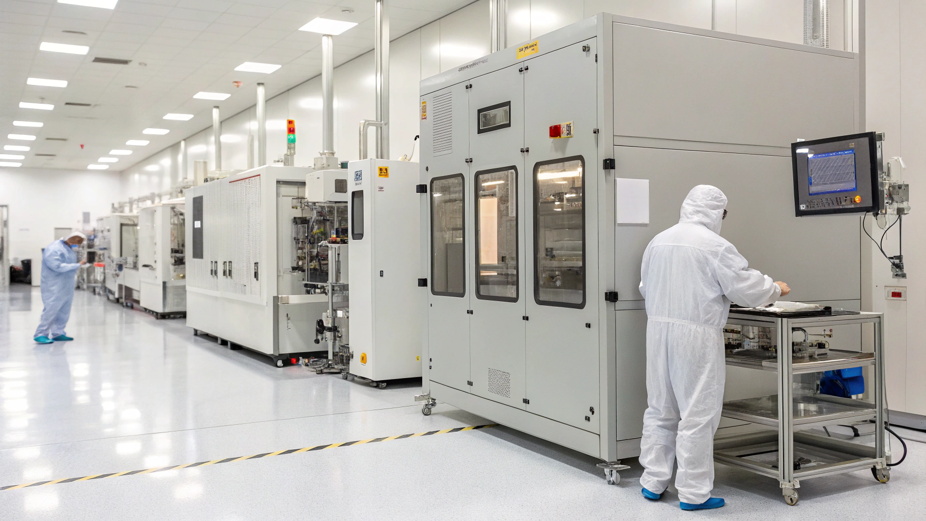
The semiconductor manufacturing process relies on various vacuum technologies and supporting equipment to maintain the required vacuum levels and ensure process stability.

Dive deeper Paragraph:
Semiconductor fabs employ sophisticated vacuum systems tailored to specific process requirements:
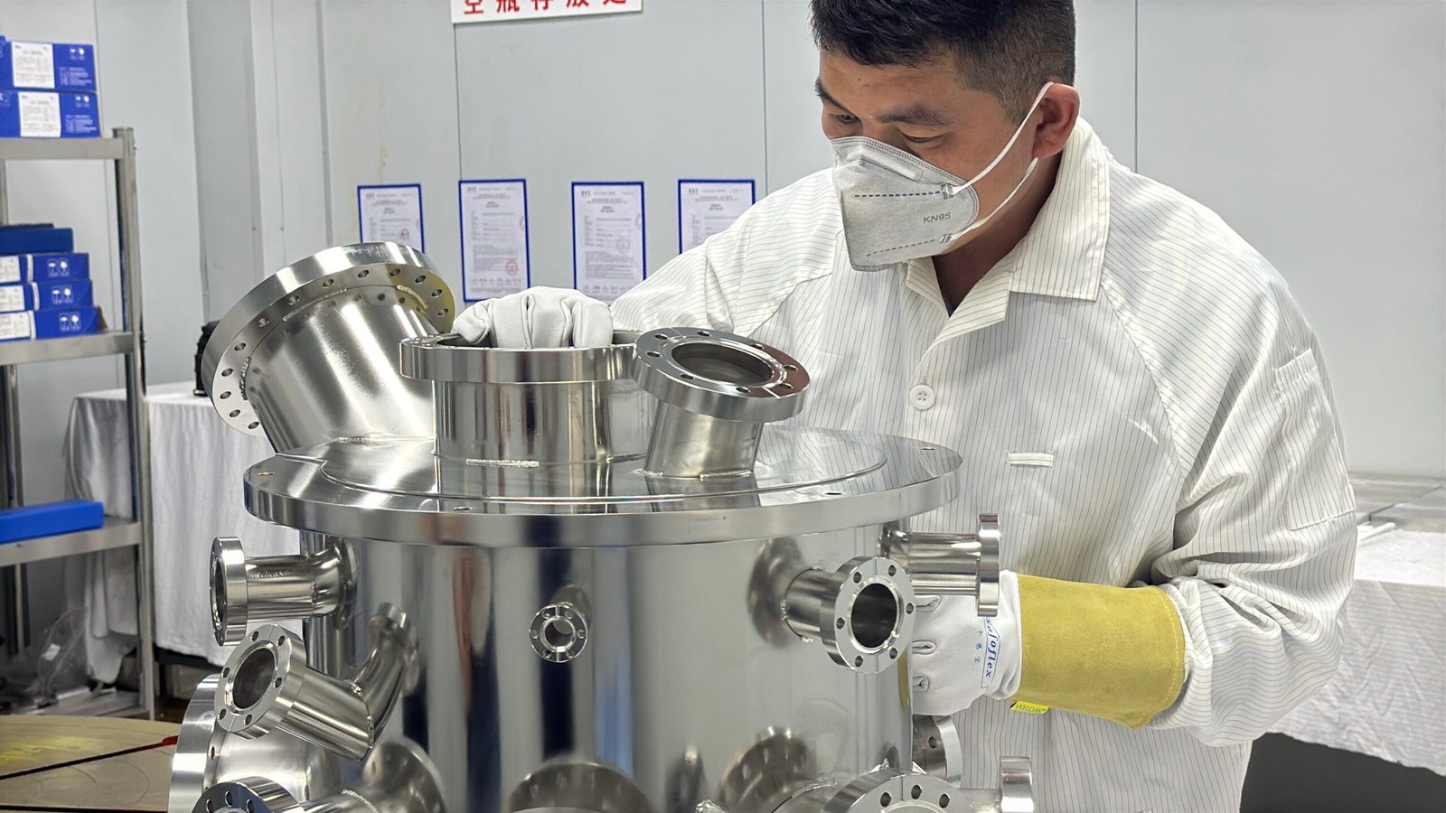
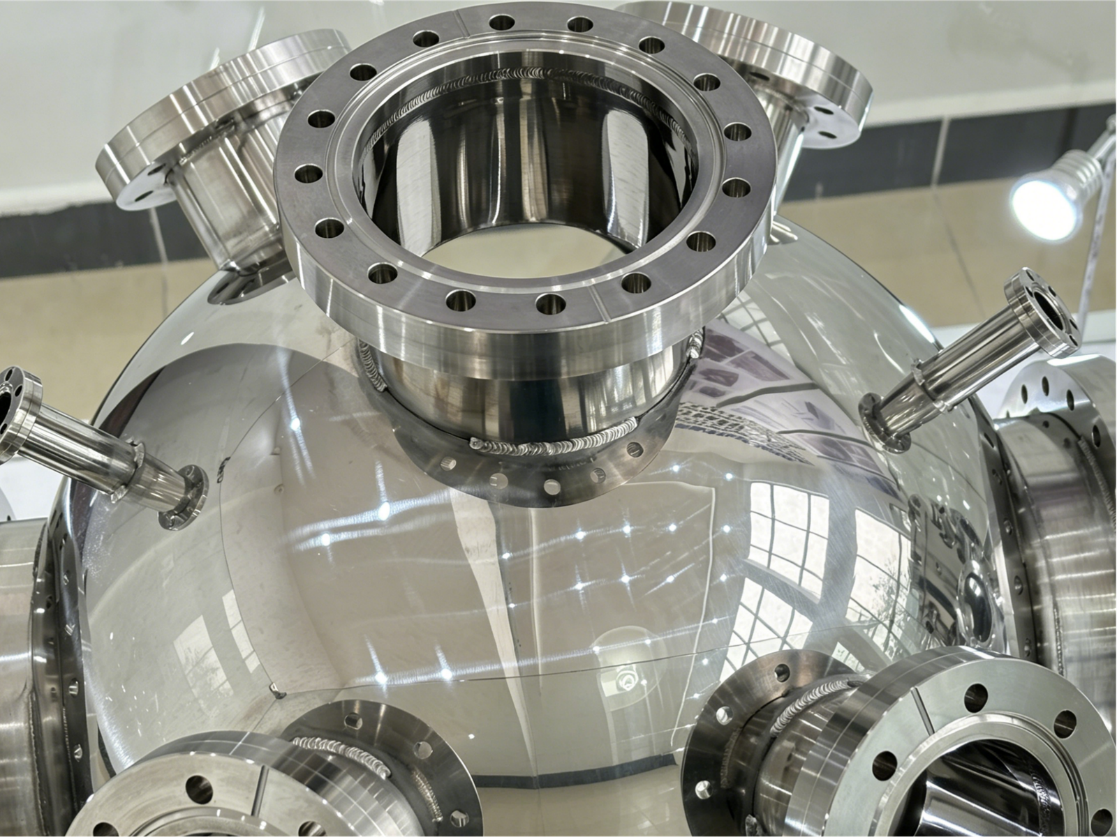
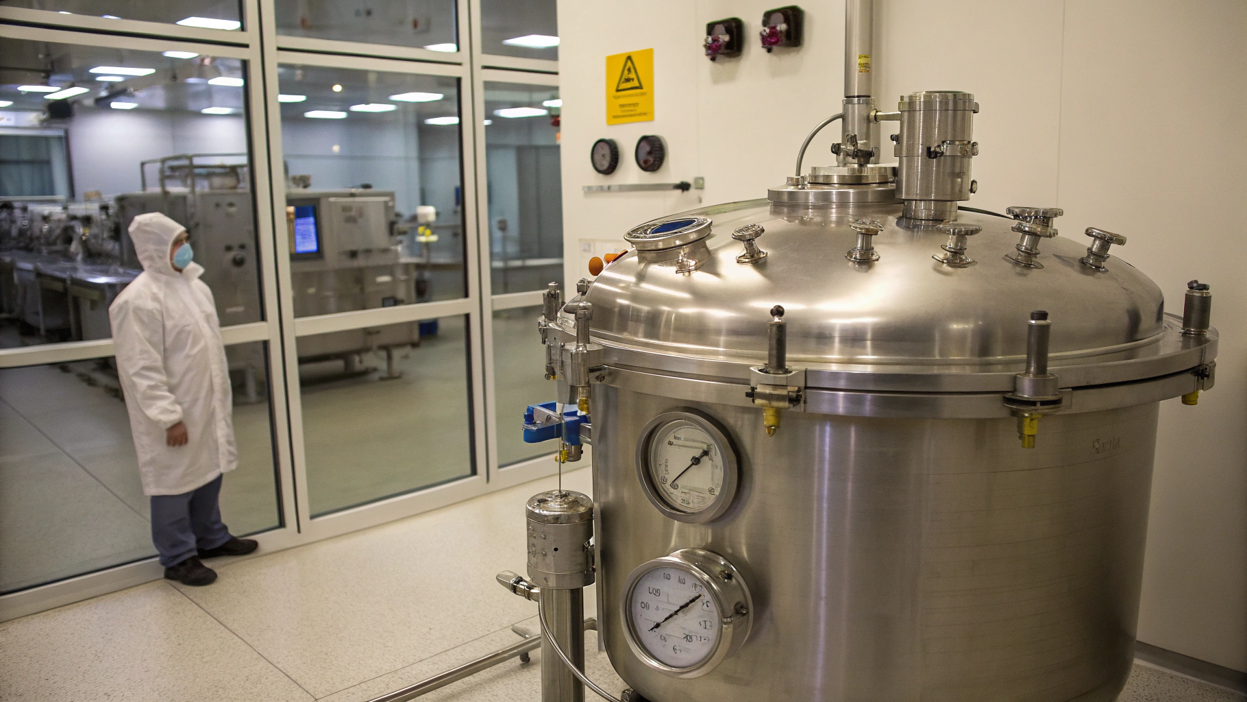
Vacuum chambers are the foundation, designed from materials with low outgassing properties like electropolished stainless steel, aluminum, or ceramics. These chambers incorporate sophisticated sealing technologies, with metal seals often preferred in UHV systems due to their lower outgassing rates compared to elastomeric seals.
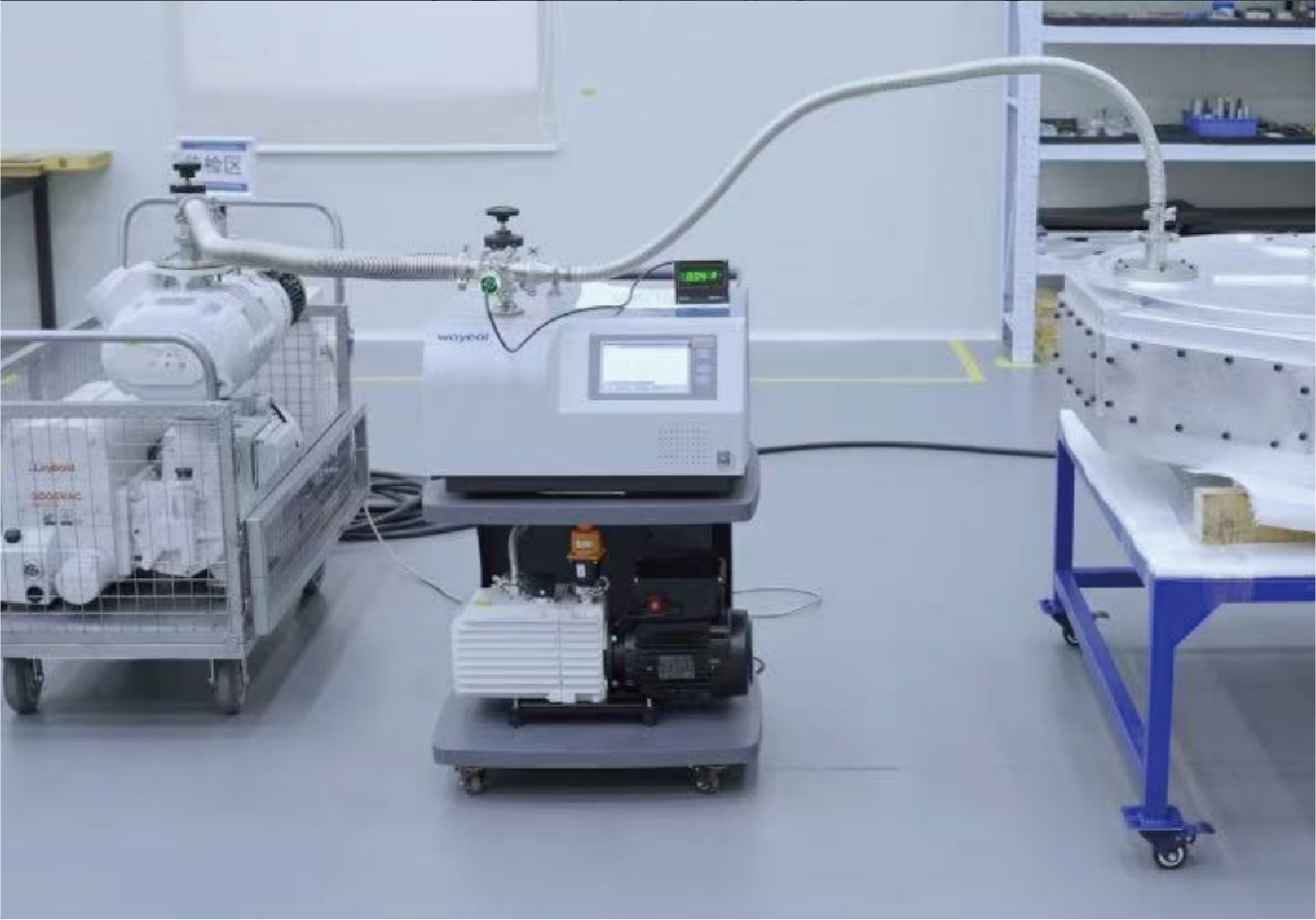
Different pump technologies work in tandem to achieve and maintain required vacuum levels:
- Mechanical pumps (including dry pumps and scroll pumps) handle the initial rough vacuum stages.
- Turbomolecular pumps serve as the workhorses for high vacuum applications, using high-speed rotating turbine blades to extract gas molecules.
- Ion pumps, commonly deployed in ultra-high vacuum systems, ionize gas molecules and accelerate them to surfaces where they're adsorbed.
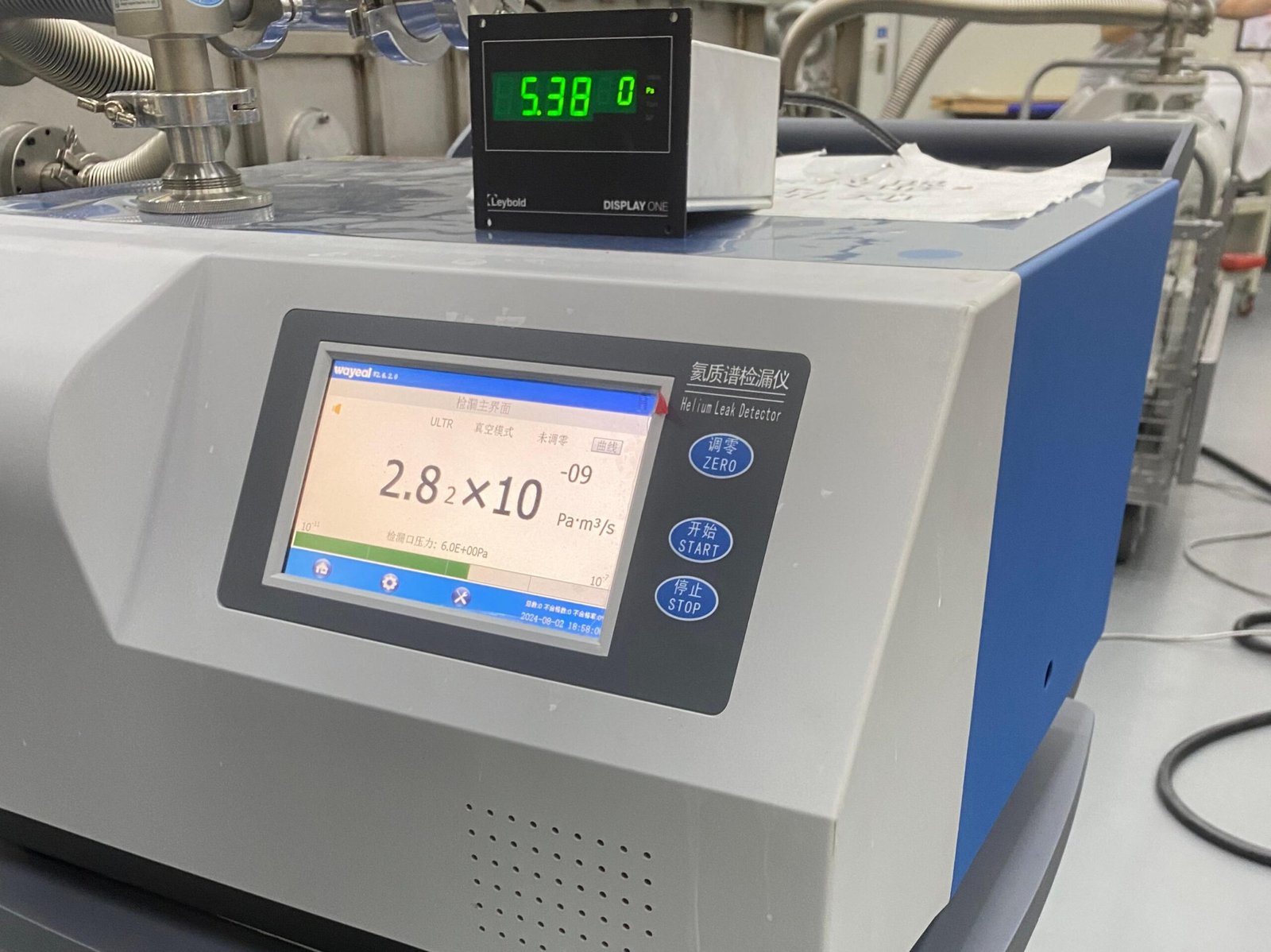
Vacuum transfer systems maintain environment integrity during wafer movement between process chambers through automated, sealed mechanisms. Precision vacuum measurement is equally critical, with ionization gauges typically used in UHV conditions due to their sensitivity to extremely low pressures.
What are the requirements for vacuum stability and purity?
In my experience, achieving high vacuum is only half the battle - maintaining stable conditions consistently is what separates successful semiconductor manufacturing from costly failures.
In precision manufacturing, the long-term stability of the vacuum environment is critical. A stable vacuum system maintains consistent process conditions and avoids product inconsistencies during manufacturing.
Dive deeper Paragraph:
The semiconductor industry imposes exceptional demands on vacuum stability and purity. Modern fabrication processes operate within strict parameter windows that must be maintained throughout the entire manufacturing cycle. Vacuum stability directly impacts critical dimensions (CD) control, with pressure fluctuations potentially causing variations in etch rates, deposition thickness, and feature geometry. For advanced nodes below 10nm, vacuum stability tolerances may be as tight as ±1% of the setpoint.
Material selection plays a crucial role in vacuum system design. Materials used in HV and UHV systems must have extremely low outgassing rates to minimize contamination and pressure increases. Surface treatments like electropolishing significantly reduce gas absorption and subsequent desorption. Vacuum systems employ sophisticated contamination control strategies, including purge cycles, cold traps, and getter materials that selectively absorb unwanted gas molecules.
Process gases introduced into vacuum chambers must meet semiconductor-grade purity specifications (often 99.9999% or better). Gas delivery systems incorporate point-of-use purifiers, mass flow controllers, and specialized monitoring equipment. The vacuum environment constantly faces challenges from process byproducts, which necessitates regular preventive maintenance and chamber cleaning protocols to maintain optimal performance and prevent cross-contamination between production batches.
Conclusion
The semiconductor industry's relentless advancement depends on sophisticated vacuum technologies tailored to each specific manufacturing process. Selecting the right vacuum technology is not merely a technical decision but a critical factor in ensuring semiconductor product quality, performance, and manufacturing yield.