Etching processes are critical in semiconductor manufacturing, requiring precisely controlled vacuum environments to ensure high precision and purity in the patterning of materials on silicon wafers 45. These specialized vacuum chambers face unique challenges while continuously benefiting from technological innovations to meet the demanding requirements of modern semiconductor fabrication.
The Fundamentals of Etching Vacuum Chambers
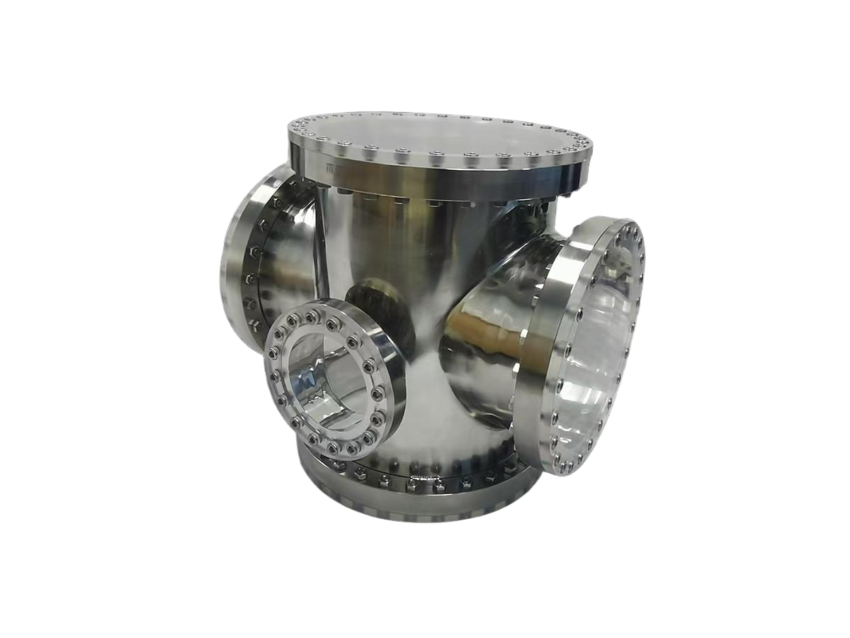
Etching vacuum chambers serve as controlled environments where materials are selectively removed from semiconductor wafers. These chambers must maintain specific vacuum levels, typically in the high vacuum (10^-3 to 10^-7 Torr) or ultra-high vacuum (below 10^-7 Torr) ranges 3. The precise vacuum level directly impacts process stability and the quality of the resulting microchips 4.
Key Challenges in Etching Vacuum Chamber Technology
1. Contamination Control
One of the most significant challenges in etching vacuum chambers is preventing contamination that could lead to defects in microchips 3. Even microscopic particles can compromise the integrity of semiconductor components, making contamination control paramount.
2. Material Selection
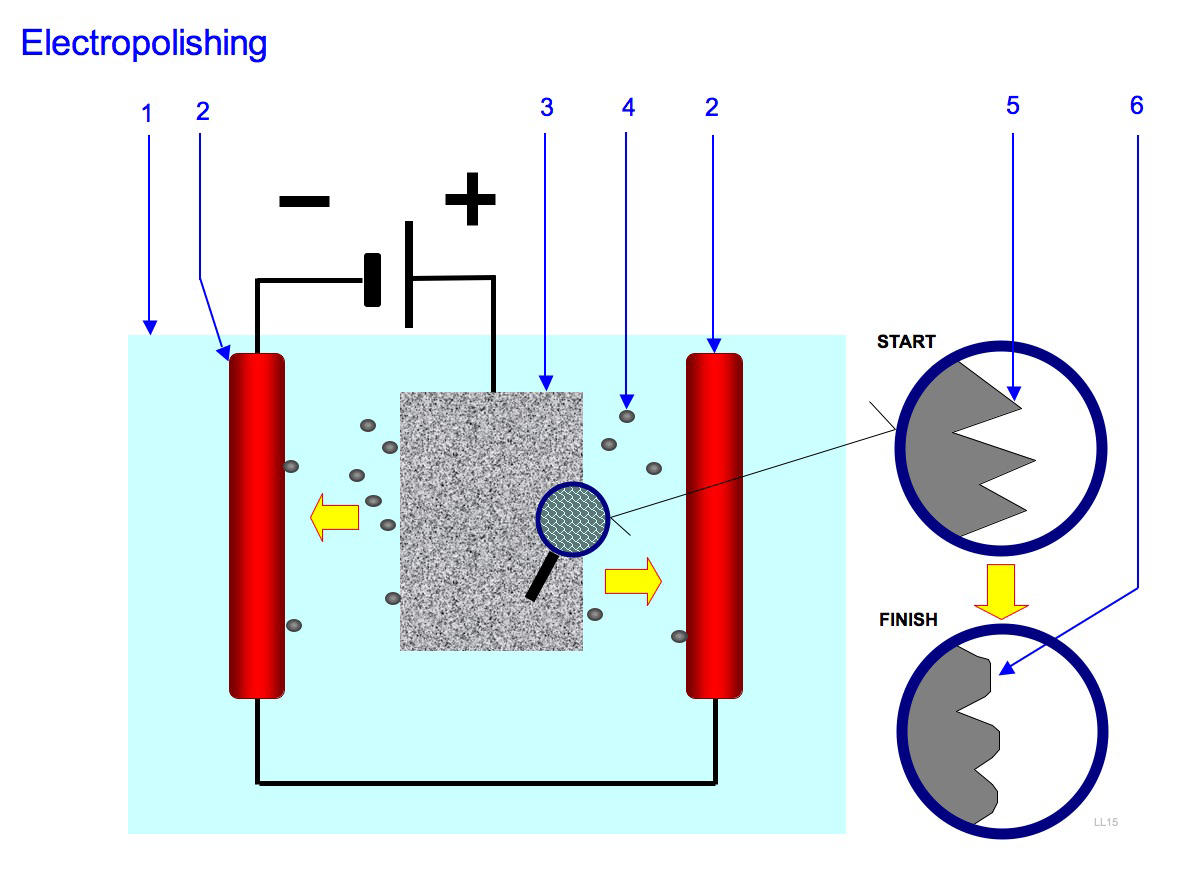
Materials used in etching vacuum chambers must have low outgassing rates to minimize contamination and pressure fluctuations. Common materials include stainless steel, aluminum, and ceramics, often with electropolished surfaces to reduce gas absorption and desorption 3.
3. Sealing Technologies
Effective sealing is critical to prevent air leakage into the vacuum environment. In high-precision etching applications, metal seals are frequently preferred over elastomeric seals due to their lower outgassing rates 3. Any compromise in sealing integrity can lead to process failures and reduced yields.
4. Pressure Stability
Maintaining stable pressure conditions throughout the etching process is essential for consistent results. This requires advanced vacuum gauge systems to monitor pressure with extreme precision, ensuring each production step operates within specified parameters 4.
5. Integration with Transfer Systems
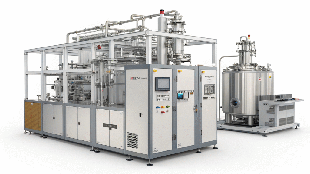
Modern semiconductor manufacturing requires materials to move between different process chambers while maintaining vacuum integrity. Developing efficient vacuum transfer systems that don't compromise the vacuum environment presents significant engineering challenges 4.
Innovations in Etching Vacuum Chamber Technology
1. Advanced Chamber Designs
Custom vacuum chamber designs now incorporate features specifically optimized for etching processes. These may include specialized port configurations, feedthroughs, and internal geometries that enhance process efficiency and uniformity 1.
2. Material and Surface Engineering
Innovations in materials science have led to vacuum chamber surfaces with significantly reduced outgassing properties. Advanced surface treatments and coatings help minimize contamination sources within the chamber itself 3.
3. Enhanced Leak Detection
Modern etching vacuum chambers benefit from advanced testing facilities, including helium mass spectrometers and ultrasonic detectors, ensuring that even microscopic leaks are identified before chambers enter production use 5.
4. Automated Monitoring Systems
Today's etching vacuum systems incorporate sophisticated pressure measurement technologies and automated monitoring systems that provide real-time data on chamber conditions, allowing for immediate adjustments to maintain optimal process parameters 4.
5. Modular Chamber Designs
Innovative modular designs allow for faster maintenance and reconfiguration of etching vacuum chambers, reducing downtime and increasing production flexibility 2.
The Future of Etching Vacuum Chamber Technology
As semiconductor device features continue to shrink, the demands on etching vacuum chambers will only increase. Future innovations will likely focus on even more precise pressure control, advanced materials with near-zero outgassing rates, and intelligent monitoring systems that can predict and prevent process deviations before they occur.
Conclusion
The technology behind etching vacuum chambers represents a critical enabler for semiconductor manufacturing advancement. By addressing the fundamental challenges of contamination control, material selection, and pressure stability while implementing innovative designs and monitoring systems, manufacturers can achieve the extreme precision required for next-generation semiconductor devices. As the industry continues to evolve, collaboration between vacuum technology specialists and semiconductor manufacturers will drive further innovations in this essential field.